Tenstorrent Guide: Blackhole RISC-V Tensix AI Architecture
The Proprietary GPU Bottleneck and Enterprise Hardware Lock-In
In modern high-throughput enterprise intelligence architectures, real-time multimodal copilot infrastructures, and autonomous agent systems powered by AI Fetchly, computational performance and serving unit economics are dictated entirely by accelerator hardware. Whether streaming autoregressive token completions from hundred-billion-parameter foundation models, extracting unstructured document payloads via automated web scraping, or executing concurrent matrix operations for real-time data ingestion, the global AI infrastructure stack is constrained by a fundamental structural bottleneck: the proprietary GPU monopoly.
For over a decade, datacenter artificial intelligence has been dominated by traditional graphics-derived compute clusters. While modern accelerators like the NVIDIA Hopper H100 and Blackwell B200 provide immense theoretical floating-point density, deploying enterprise workloads on conventional GPU architectures introduces four critical systemic failure modes that inflate operational expenditures and restrict architectural innovation:
1. The Von Neumann Host-Device Offloading Tax
Conventional GPU infrastructure relies on a rigid, master-worker offloading topology. A central host computer powered by expensive x86_64 server processors manages operating system scheduling, memory allocation, PCIe enumeration, and runtime orchestration, treating the GPU purely as an attached PCIe peripheral device.
When executing long-horizon AI agent workflows or multi-turn conversational pipelines, this partitioned hierarchy incurs substantial latency penalties:
- Every forward pass or kernel invocation requires transmitting command buffers, launch descriptors, and synchronization barriers across the PCIe bus.
- Pre-processing (tokenization, prompt normalization, formatting) and post-processing (logit filtering, sampling, greedy decoding) are repeatedly ping-ponged between host CPU system DRAM and GPU High-Bandwidth Memory (HBM).
- The host CPU becomes an unavoidable single-point bottleneck, capping cluster scaling and leaving GPU compute units idling during CPU-bound memory marshaling phases.
- In dynamic autoregressive loops, where token-by-token generation depends on immediate step-level evaluations, host-to-device round-trip latency frequently dominates execution time over raw matrix compute.
Traditional GPU Server vs. Autonomous AI Processor Architecture:
+-----------------------------------------------------------------------------------+
| LEGACY GPU SERVER: Partitioned Host-Device Offloading Model                        |
+-----------------------------------------------------------------------------------+
| [Dual x86 Host CPUs ($15k)] <--- PCIe 5.0 Bus (Bottleneck) ---> [8x H100 GPUs ($300k)] |
| - High-latency kernel dispatch and synchronization barriers                        |
| - Complex host DRAM <-> Device HBM buffer copies and PCIe serialization           |
| - Heavy dependency on proprietary closed-source driver and CUDA runtime blobs     |
+-----------------------------------------------------------------------------------+
| TENSTORRENT BLACKHOLE: Sovereign Autonomous AI Computing Node                     |
+-----------------------------------------------------------------------------------+
| [On-Die 16x SiFive x280 RISC-V CPUs] <--- Ultra-Fast NoC ---> [120 Tensix Cores]    |
| - Standalone Linux host boots natively on-chip; eliminates external x86 servers   |
| - Direct zero-overhead kernel launch and packetized SRAM-to-SRAM transfers        |
| - 100% open-source software stack: TT-Metalium, TT-NN, and TT-Forge (Apache 2.0)   |
+-----------------------------------------------------------------------------------+ 2. Packaging Bottlenecks and High-Bandwidth Memory Fragility
To feed hungry matrix multiplication engines with tens of terabytes per second of raw data throughput, frontier GPUs rely exclusively on High-Bandwidth Memory (HBM3e). While HBM provides extraordinary burst bandwidth (exceeding 3 TB/s per package), it requires advanced 2.5D wafer-level multi-chip packaging, such as TSMC Chip-on-Wafer-on-Substrate (CoWoS):
- Manufacturing Fragility: Advanced silicon interposers and microscopic microbump arrays suffer from constrained global foundry capacity, creating massive supply chain shortages and lead times exceeding 9 to 12 months.
- Prohibitive Bill of Materials: The physical HBM stacks and interposers frequently account for more than 50% to 60% of the raw bill of materials (BOM) cost of an accelerator module, driving retail accelerator prices past $30,000 to $40,000 per board.
- Thermal Density Constraints: Stacking dynamic RAM dies directly adjacent to high-power logic dies creates intense thermal coupling, requiring complex liquid cooling loops and elevating failure rates in enterprise datacenters.
- Yield Sensitivity: If a single microscopic microbump fails across the multi-die substrate, the entire multi-thousand-dollar package must be scrapped, driving up effective silicon wafer waste.
3. The Proprietary Software Moat and Vendor Lock-In
For software engineers and infrastructure architects, the greatest barrier in accelerated computing is software lock-in. Datacenter hardware has historically been chained to proprietary, closed-source compiler chains, closed-source firmware, and vendor-specific runtime libraries:
- Proprietary CUDA runtimes obscure hardware execution mechanics, making low-level compiler optimization, custom memory tiering, and non-standard tensor abstractions exceptionally difficult.
- Custom silicon architectures from competing vendors frequently fail because their software ecosystems require years of reverse engineering and brittle translation layers.
- Developers are left unable to inspect hardware registers, optimize custom attention patterns, or build specialized execution graphs without waiting for proprietary upstream vendor updates.
- Enterprises face vendor lock-in that prevents migrating mission-critical workloads to alternative hardware architectures, cementing inflated datacenter margins.
4. Rigid Multi-Node Networking Overhead
Scaling out GPU clusters to thousands of devices requires layering expensive external networking fabrics on top of server chassis:
- PCIe-attached NICs (such as ConnectX-7 InfiniBand or RoCE adapters) require additional PCIe switches, retimers, optical transceivers, and dedicated spine-leaf networking fabrics.
- Remote Direct Memory Access (RDMA) transfers between nodes must navigate a labyrinthine path: GPU HBM -> PCIe Switch -> Host Root Complex -> PCIe NIC -> Optical Transceiver -> Top-of-Rack Switch -> Target Node.
- This layered topology introduces significant latency variance, packet jitter, and catastrophic tail latencies during distributed all-reduce and tensor parallelism operations.
- The networking infrastructure alone can add up to 30% of the capital expenditure of a modern AI supercluster, accompanied by substantial power overhead from external switches.
The Tenstorrent Paradigm: RISC-V, Tensix Cores, and Native Silicon Autonomy
To systematically dismantle the GPU monopoly and establish an open, cost-effective computing foundation, microprocessor legend Jim Keller (lead architect of AMD Zen, Apple K7/K8, and Tesla Autopilot hardware) founded and leads Tenstorrent. The company’s architectural philosophy is rooted in a radical rethink of accelerated computing: combine open-source RISC-V flexibility, high-density matrix-vector engines, software-driven packetized networking, and native silicon autonomy.
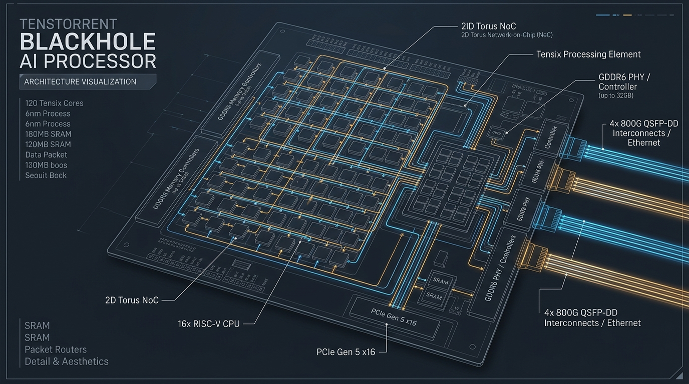
Tenstorrent Blackhole Architectural Blueprint:
+------------------------------------------------------------------------------------+
| TENSTORRENT BLACKHOLE PROCESSOR ARCHITECTURE (TSMC 6nm, 300W TBP)                   |
+------------------------------------------------------------------------------------+
|                                                                                    |
|  +------------------------------------------------------------------------------+  |
|  | 16x On-Die "Big RISC-V" Application CPU Cores (SiFive Intelligence X280)    |  |
|  | - 64-bit multi-core SMP Linux host subsystem; runs Ubuntu 22.04 on-chip      |  |
|  | - 512-bit RISC-V Vector (RVV) extensions for general preprocessing/control   |  |
|  +------------------------------------------------------------------------------+  |
|                                        |                                           |
|                   ============================================                     |
|                   2D Bi-Directional Torus Network-on-Chip (NoC)                    |
|                   ============================================                     |
|                   |                    |                     |                     |
|  +--------------------+  +--------------------+   +--------------------+           |
|  | Tensix Core (0, 0) |  | Tensix Core (0, 1) |...| Tensix Core (X, Y) |           |
|  | - 5x Baby RISC-Vs  |  | - 5x Baby RISC-Vs  |   | - 5x Baby RISC-Vs  |           |
|  | - MatMul FPU Array |  | - MatMul FPU Array |   | - MatMul FPU Array |           |
|  | - Vector SIMD Unit |  | - Vector SIMD Unit |   | - Vector SIMD Unit |           |
|  | - 1.5 MB L1 SRAM   |  | - 1.5 MB L1 SRAM   |   | - 1.5 MB L1 SRAM   |           |
|  +--------------------+  +--------------------+   +--------------------+           |
|         (120 Functional Tensix Compute Cores = 180 MB Total On-Chip SRAM)          |
|                                                                                    |
|  +--------------------------+  +--------------------------+  +------------------+  |
|  | 32 GB Standard GDDR6     |  | 4x 800G QSFP-DD Ports    |  | PCIe 5.0 x16     |  |
|  | 256-bit Bus, 512 GB/s BW |  | Native Optical Scale-Out |  | Host/Device Bus  |  |
|  +--------------------------+  +--------------------------+  +------------------+  |
+------------------------------------------------------------------------------------+ 1. Eliminating the Host CPU: Sovereign On-Chip Linux Execution
Unlike traditional GPUs that require an external host server to boot, dispatch, and monitor execution, the Tenstorrent Blackhole processor embeds 16 SiFive Intelligence X280 “Big RISC-V” 64-bit application CPU cores directly on the silicon die:
- The chip boots a complete, standard Linux operating system (such as Ubuntu 22.04 LTS) natively.
- The 16 X280 cores run standard software utilities, network daemons, Python runtimes, and PyTorch execution loops directly on-chip.
- Peripheral tokenization, context buffering, and API serving are executed internally, completely eliminating the PCIe host-device latency bottleneck. A Blackhole card can function as a standalone, sovereign computing node requiring only power and network cabling.
- The X280 application cluster features 512-bit RISC-V Vector (RVV) extensions, allowing it to perform high-speed SIMD scalar preprocessing, data parsing, and string manipulation without touching the matrix cores.
2. Commodity GDDR6 Memory with Massive Cost Advantages
Instead of incurring the astronomical packaging and supply chain overhead of HBM, Blackhole utilizes standard, high-yield GDDR6 memory:
- Operates a 256-bit memory subsystem delivering up to 512 GB/s of sustained memory bandwidth (16 GT/s) with 32 GB of capacity on the Blackhole p150a and p150b cards (and 28 GB on the evaluation p100a).
- Standard monolithic silicon manufacturing on TSMC 6nm avoids CoWoS interposers, slashing production costs to a fraction of GPU modules while ensuring massive, uninterrupted foundry availability.
- The 32 GB GDDR6 capacity allows deploying dense 8B models (such as LLaMA-3.1-8B) or serving quantized 70B MoE layers locally at standard server power envelopes.
- Commodity GDDR6 memory controllers benefit from mature desktop graphics and gaming console supply chains, avoiding the volatile pricing spikes of datacenter memory.
3. Integrated Native Optical Networking (Glueless Scale-Out)
Blackhole integrates dedicated network hardware directly into the silicon logic:
- Each Blackhole p150 card features four passive 800 Gbps QSFP-DD ports, providing an aggregate 3.2 Terabits per second (Tbps) of direct optical inter-chip networking.
- Cables plug directly from one Blackhole card into another without requiring external Ethernet switches, InfiniBand directors, or PCIe network interface cards.
- The on-chip Network-on-Chip (NoC) seamlessly extends across optical cables, allowing Tensix cores on Card A to write directly into the L1 SRAM of Tensix cores on Card B across datacenter racks.
- Eliminating external network switches reduces cluster transit latency by hundreds of nanoseconds, fundamentally transforming all-gather and reduce-scatter operations.
Deep Dive: The Tensix Core & 2D Toroidal Network-on-Chip
At the heart of Tenstorrent’s computing capability is the Tensix Core—a highly optimized, programmable processing tile designed specifically for linear algebra, activation functions, and asynchronous data streaming.
1. Anatomy of a Tensix Processing Tile
In Blackhole, the silicon die integrates an array of Tensix cores, with 120 fully functional compute cores enabled on production cards (providing 180 MB of ultra-fast on-chip SRAM at 1.5 MB per core).
Each Tensix core is not a rigid systolic array; it is a complete, multi-threaded computing node containing:
- Five “Baby RISC-V” Cores: Dedicated microcontrollers that manage data movement and arithmetic scheduling concurrently:
- Unpack 0 and Unpack 1: Dedicated RISC-V cores responsible for reading data from local L1 SRAM or the NoC, decompressing block floating-point representations, and feeding them into the compute pipeline.
- Math RISC: Orchestrates the matrix and vector execution units, issuing instructions to the tensor FPU and vector SIMD engines.
- Pack: Converts high-precision mathematical results into compressed output formats (e.g., FP8, BFP8, FP16) and commits them back to L1 SRAM.
- Router / Movement RISC: Manages asynchronous packet transmission across the 2D Torus NoC.
- Matrix Multiplication Engine (FPU): High-density arithmetic array optimized for outer-product matrix multiply-accumulate operations, delivering up to 664 TeraFLOPS of BLOCKFP8 tensor compute at 1.35 GHz.
- Vector SIMD Engine: High-performance vector processing unit dedicated to element-wise operations, activations (GELU, SiLU, ReLU), LayerNorm, and softmax reductions.
- 1.5 MB Local L1 SRAM: Ultra-low-latency scratchpad memory accessible by local execution units with single-cycle latency, eliminating register-spill stalls.
Detailed Microarchitecture of a Single Tensix Processing Tile:
+------------------------------------------------------------------------------------+
| TENSIX CORE ARCHITECTURAL SCHEMATIC                                                |
+------------------------------------------------------------------------------------+
|                                                                                    |
|   +----------------------------------------------------------------------------+   |
|   | 1.5 MB Local L1 High-Bandwidth SRAM Scratchpad Memory                      |   |
|   +----------------------------------------------------------------------------+   |
|         ^                                                             |            |
|         | Data Packets                                                | Unpack     |
|   +---------------+                                            +---------------+   |
|   | Pack RISC-V   |                                            | Unpack RISC-V |   |
|   | Micro-Engine  |                                            | (0 & 1 Engines|   |
|   +---------------+                                            +---------------+   |
|         ^                                                             |            |
|         | Formatted Results                                           | Operands   |
|   +----------------------------------------------------------------------------+   |
|   | MATH & COMPUTE PIPELINE (Orchestrated by Math RISC-V Core)                 |   |
|   |                                                                            |   |
|   |  +----------------------------------+  +--------------------------------+  |   |
|   |  | Dense Matrix Multiply FPU Array  |  | Vector SIMD Engine             |  |   |
|   |  | - BLOCKFP2/4/8, FP8, FP16, BF16  |  | - Softmax, LayerNorm, GELU/SiLU|  |   |
|   |  | - TF32, INT8 Tensor Compute      |  | - Element-wise Math, Reductions|  |   |
|   |  +----------------------------------+  +--------------------------------+  |   |
|   +----------------------------------------------------------------------------+   |
|         ^                                                             ^            |
|         |                                                             |            |
|   +----------------------------------------------------------------------------+   |
|   | 2D Torus Network-on-Chip (NoC) Interface & Packet Router                   |   |
|   | - Bi-directional X/Y Ring Buffers (North, South, East, West Channels)      |   |
|   +----------------------------------------------------------------------------+   |
|                                                                                    |
+------------------------------------------------------------------------------------+ 2. Cycle-by-Cycle Execution and Circular Buffering Mechanics
To achieve maximum computational efficiency, Tensix cores rely on an asynchronous, pipelined dataflow model governed by Circular Buffers (CBs) allocated inside local L1 SRAM.
In conventional GPU architectures, thread warps frequently stall on memory access when loading data from global HBM into shared memory (SRAM), requiring hundreds of active threads to hide memory latency. In contrast, Tenstorrent decouples data movement from mathematical computation entirely:
- Asynchronous Double Buffering: L1 SRAM is partitioned into circular buffers configured with multiple pages. While the Math RISC core executes matrix operations on Page 0, the Unpack RISC cores independently fetch the next matrix tile from GDDR6 or remote Tensix tiles into Page 1 via the NoC.
- Hardware Semaphore Synchronization: The Baby RISC cores coordinate through lightweight hardware semaphores. When the Unpack engine finishes transferring a tile, it increments an input semaphore (
cb_push_back). The Math engine consumes the tile, executes the FPU operations, and decrements the semaphore (cb_pop_front), alerting the memory engines to refill the buffer. - Zero Compute Interruption: Because data prefetching operates concurrently and independently of the arithmetic units, the matrix FPU runs at near 100% saturation without pipeline bubbles or execution stalls.
$$ \text{Throughput} = \frac{\text{Tiles}{\text{computed}}}{\text{Cycles}{\text{total}}} \approx \min\left(1.0, \frac{\text{Bandwidth}{\text{NoC}}}{\text{Compute}{\text{FPU}}} ight) $$
3. The 2D Bi-Directional Toroidal Network-on-Chip (NoC)
Traditional multi-core processors connect computing tiles via crossbar switches or mesh networks that experience severe contention under non-local traffic. Tenstorrent implements a 2D Bi-Directional Toroidal Network-on-Chip (NoC):
- Cores are organized in a 2D grid with ring connections along rows (East-West) and columns (North-South), with wrap-around links forming a torus.
- The interconnect operates on packetized data streams: cores do not issue blocking load/store memory operations across the chip; instead, data is pushed asynchronously in structured packets.
- The NoC features dedicated hardware routers that forward packets without interrupting active compute execution, achieving deterministic latency and massive aggregate cross-sectional bandwidth across the 180 MB SRAM substrate.
- Each Tensix core exposes two independent NoC endpoints (NoC0 and NoC1), enabling simultaneous transmission of incoming activation tiles and outgoing gradient or result packets.
4. Data Formats and Numerical Precision Flexibility
Blackhole provides extraordinary data precision flexibility across both Tensix compute engines and the SiFive x280 application subsystem:
| Numeric Format Family | Supported Precision on Tensix Cores | Supported Precision on Big RISC-V Cores | Architectural Application |
|---|---|---|---|
| Standard Floating-Point | FP8 (E4M3, E5M2), FP16, BFLOAT16, FP32 (Output) | FP8, FP16, BFLOAT16, FP32, FP64 | Frontier LLM Pre-training & Serving |
| Block Floating-Point | BLOCKFP2, BLOCKFP4, BLOCKFP8 | N/A (Emulated in software) | Ultra-dense quantization & 664 TFLOPS peak compute |
| Integer Arithmetic | INT8, INT32 (Accumulator Output) | INT8, INT16, INT32, INT64 | Classical computer vision & quantized embeddings |
| TensorFloat Precision | TF32 (19-bit dynamic range) | N/A | High-precision scientific & finance simulations |
| Vector SIMD Precision | VTF19, VFP32 | VFP64 (64-bit IEEE 754) | LayerNorm, Softmax, RoPE positional encoding |
The support for Block Floating-Point (BFP) is particularly significant. In BFP formats (such as BLOCKFP8), a shared exponent is computed across an entire 16x16 or 32x32 tensor tile, while individual mantissas are stored as compact 8-bit, 4-bit, or 2-bit integers. This technique slashes memory bandwidth requirements by up to 75% compared to standard floating point while retaining full dynamic range across wide gradient distributions.
Software Stack & Bare-Metal Programming with TT-Metalium
A revolutionary semiconductor architecture is worthless without an accessible, productive software stack. Tenstorrent rejects proprietary vendor runtimes in favor of a completely open-source, multi-tiered software ecosystem (licensed under Apache 2.0).
The Open-Source Tenstorrent Software Hierarchy:
+-----------------------------------------------------------------------------------+
| APPLICATION LAYER: Hugging Face, PyTorch, vLLM, ONNX Runtime                      |
+-----------------------------------------------------------------------------------+
                                         |
+-----------------------------------------------------------------------------------+
| TT-FORGE: High-Level Graph Compiler (PyTorch / ONNX / XLA Graph Ingestion)        |
| - Automatic graph partitioning, tensor sharding, and memory layout scheduling     |
+-----------------------------------------------------------------------------------+
                                         |
+-----------------------------------------------------------------------------------+
| TT-NN: High-Performance Neural Network Operator Library                           |
| - Optimized transformer layers, Multi-Head Latent Attention, FlashAttention, RMSNorm |
+-----------------------------------------------------------------------------------+
                                         |
+-----------------------------------------------------------------------------------+
| TT-METALIUM: Bare-Metal C++ Low-Level Kernel & Tensor Programming API             |
| - Explicit circular buffer allocation, NoC data movement, and thread execution    |
+-----------------------------------------------------------------------------------+
                                         |
+-----------------------------------------------------------------------------------+
| HARDWARE SILICON: Blackhole p150 Tensix Processors & SiFive RISC-V Subsystem       |
+-----------------------------------------------------------------------------------+ 1. Understanding the TT-Metalium Execution Model
TT-Metalium is Tenstorrent’s low-level C++ programming interface—the open-source equivalent to NVIDIA CUDA or Triton. In TT-Metalium, programmers write high-performance kernels by explicitly orchestrating:
- Host Program (
host.cpp): Allocates device memory buffers (DRAM or L1 SRAM), configures circular buffers (CBs), and launches kernels across a specified grid of Tensix cores. - Data Movement Kernels (
reader.cpp,writer.cpp): Executed by the Unpack and Pack RISC-V micro-engines to stream tiles from DRAM across the NoC into local L1 circular buffers. - Compute Kernel (
compute.cpp): Executed by the Math RISC-V micro-engine, invoking hardware-accelerated tensor math primitives (matmul_tiles,add_tiles,gelu_tile). - Memory Layout Abstractions: TT-Metalium natively supports multiple tensor storage layouts:
- Interleaved Layout: Data tiles are striped evenly across all GDDR6 memory channels to maximize external bandwidth.
- Sharded Layout: Tensors are pinned directly into the L1 SRAM of specific Tensix cores, enabling zero-copy local computation.
- Tile Layout: Data is organized into 32x32 element tiles matching Tensix hardware registers, avoiding strided memory transposition penalties.
2. Concrete Implementation: Writing a Matrix Multiplication Kernel in TT-Metalium
Below is a complete, production-grade example illustrating how to define, configure, and launch a tiled Matrix Multiplication kernel on Blackhole Tensix cores using C++ and TT-Metalium:
// ============================================================================
// File: tt_metalium_matmul_example.cpp
// Description: Tiled Matrix Multiplication on Tenstorrent Blackhole Tensix Cores
// Architecture: TT-Metalium Bare-Metal Kernel Pipeline
// ============================================================================

#include "tt_metal/host_api.hpp"
#include "tt_metal/common/constants.hpp"
#include "tt_metal/detail/util.hpp"

using namespace tt::tt_metal;

int main(int argc, char** argv) {
    // 1. Initialize Device and Command Queue
    constexpr int device_id = 0;
    Device* device = CreateDevice(device_id);
    CommandQueue& cq = device->command_queue();

    // 2. Define Matrix Dimensions (Tiled into 32x32 Sub-blocks)
    constexpr uint32_t M = 1024; // Batch / Sequence Length
    constexpr uint32_t K = 2048; // Hidden Dimension In
    constexpr uint32_t N = 1024; // Hidden Dimension Out

    constexpr uint32_t TILE_WIDTH = 32;
    constexpr uint32_t TILE_HEIGHT = 32;
    constexpr uint32_t num_tiles_M = M / TILE_HEIGHT;
    constexpr uint32_t num_tiles_K = K / TILE_WIDTH;
    constexpr uint32_t num_tiles_N = N / TILE_WIDTH;

    // 3. Allocate Interleaved GDDR6 Buffers for Inputs A, B, and Output C
    constexpr uint32_t tile_size_bytes = 2 * 32 * 32; // BFLOAT16: 2048 bytes
    InterleavedBufferConfig dram_config{
        .device = device,
        .size = num_tiles_M * num_tiles_K * tile_size_bytes,
        .page_size = tile_size_bytes,
        .buffer_type = BufferType::DRAM
    };
    std::shared_ptr<Buffer> src0_dram = CreateBuffer(dram_config);
    dram_config.size = num_tiles_K * num_tiles_N * tile_size_bytes;
    std::shared_ptr<Buffer> src1_dram = CreateBuffer(dram_config);
    dram_config.size = num_tiles_M * num_tiles_N * tile_size_bytes;
    std::shared_ptr<Buffer> dst_dram = CreateBuffer(dram_config);

    // 4. Construct the TT-Metalium Program and Compute Grid
    Program program = CreateProgram();
    CoreCoord core_start = {0, 0};
    CoreCoord core_end = {7, 7}; // Use an 8x8 Tensix Core Grid (64 Cores)
    CoreRange core_range(core_start, core_end);
    CoreRangeSet core_grid({core_range});

    // 5. Configure Double-Buffered L1 Circular Buffers (CBs)
    constexpr uint32_t cb_src0_index = CB::c_in0;
    constexpr uint32_t cb_src1_index = CB::c_in1;
    constexpr uint32_t cb_output_index = CB::c_out0;

    CircularBufferConfig cb_src0_cfg = CircularBufferConfig(
        2 * tile_size_bytes, {{cb_src0_index, tt::DataFormat::Float16_b}}
    ).set_page_size(cb_src0_index, tile_size_bytes);
    CreateCircularBuffer(program, core_grid, cb_src0_cfg);

    CircularBufferConfig cb_src1_cfg = CircularBufferConfig(
        2 * tile_size_bytes, {{cb_src1_index, tt::DataFormat::Float16_b}}
    ).set_page_size(cb_src1_index, tile_size_bytes);
    CreateCircularBuffer(program, core_grid, cb_src1_cfg);

    CircularBufferConfig cb_out_cfg = CircularBufferConfig(
        2 * tile_size_bytes, {{cb_output_index, tt::DataFormat::Float16_b}}
    ).set_page_size(cb_output_index, tile_size_bytes);
    CreateCircularBuffer(program, core_grid, cb_out_cfg);

    // 6. Compile and Bind Data-Movement Kernels (Unpack / Pack RISC-Vs)
    auto reader_kernel = CreateKernel(
        program,
        "kernels/dataflow/reader_bmm_interleaved.cpp",
        core_grid,
        DataMovementConfig{
            .processor = DataMovementProcessor::RISCV_0, // Unpack Engine
            .noc = NOC::RISCV_0_default
        }
    );

    auto writer_kernel = CreateKernel(
        program,
        "kernels/dataflow/writer_bmm_interleaved.cpp",
        core_grid,
        DataMovementConfig{
            .processor = DataMovementProcessor::RISCV_1, // Pack Engine
            .noc = NOC::RISCV_1_default
        }
    );

    // 7. Compile and Bind Matrix Math Kernel (Compute Engine)
    std::vector<uint32_t> compute_args = {num_tiles_M, num_tiles_K, num_tiles_N};
    auto matmul_kernel = CreateKernel(
        program,
        "kernels/compute/bmm_large_block.cpp",
        core_grid,
        ComputeConfig{
            .math_fidelity = MathFidelity::HiFi4,
            .fp32_dest_acc_en = false,
            .compile_args = compute_args
        }
    );

    // 8. Enqueue Execution and Synchronize
    EnqueueProgram(cq, program, false);
    Finish(cq);

    // Clean up
    CloseDevice(device);
    return 0;
} 3. High-Level Python Serving via TT-NN and PyTorch
For application developers who do not require low-level C++ kernel authoring, Tenstorrent provides TT-NN—a high-level, tensor-centric Python library that integrates directly with PyTorch models and Hugging Face pipelines:
# ============================================================================
# File: tt_nn_llama_inference.py
# Description: Serving LLaMA-3.1 Layers on Tenstorrent Blackhole via TT-NN
# ============================================================================

import torch
import ttnn

def serve_tenstorrent_llama():
    # 1. Open Blackhole Hardware Accelerator Device
    device_id = 0
    device = ttnn.open_device(device_id=device_id)

    # 2. Allocate Tensors in Host PyTorch Memory
    batch_size = 1
    seq_len = 2048
    hidden_dim = 4096
    intermediate_dim = 14336

    # Simulated input activations and gate weights
    x_host = torch.randn(batch_size, seq_len, hidden_dim, dtype=torch.bfloat16)
    w_gate_host = torch.randn(hidden_dim, intermediate_dim, dtype=torch.bfloat16)

    # 3. Interleave and Shard Tensors onto Blackhole GDDR6 / L1 SRAM
    # ttnn.TILE_LAYOUT organizes data into native 32x32 Tensix hardware tiles
    x_device = ttnn.from_torch(
        x_host,
        dtype=ttnn.bfloat16,
        layout=ttnn.TILE_LAYOUT,
        device=device
    )
    w_gate_device = ttnn.from_torch(
        w_gate_host,
        dtype=ttnn.bfloat16,
        layout=ttnn.TILE_LAYOUT,
        device=device
    )

    # 4. Execute Native GEMM on 120 Tensix Cores
    # Hardware runs asynchronously via packetized NoC data transfers
    gate_out = ttnn.linear(x_device, w_gate_device)

    # 5. Execute Fused Activation (SiLU Element-Wise Operation)
    activated_gate = ttnn.silu(gate_out)

    # 6. Retrieve Results Back to Host Tensor
    result_host = ttnn.to_torch(activated_gate)
    print("Execution Successful! Result Shape:", result_host.shape)

    # 7. Cleanly release accelerator context
    ttnn.close_device(device)

if __name__ == "__main__":
serve_tenstorrent_llama() Architectural Comparison: Tenstorrent Blackhole vs. Modern AI Accelerators
To contextualize Tenstorrent Blackhole against the modern landscape of high-performance AI silicon, we evaluate its physical architecture, memory subsystems, host dependencies, and cluster topologies against leading competitors:
+----------------------------------------------------------------------------------------------------+
| DATACENTER ACCELERATOR COMPARATIVE SPECS (2026 PRODUCTION SYSTEMS)                                 |
+----------------------------------------------------------------------------------------------------+
| Metric / Feature          | NVIDIA H100 SXM5      | Groq LPU (GroqCard)  | Tenstorrent Blackhole p150 |
+---------------------------+-----------------------+----------------------+----------------------------+
| Core Architecture         | 132 SMs (SIMT GPUs)   | 1x Large TSP Core    | 120 Tensix (RISC-V Tiles)  |
| On-Die CPU Host Subsystem | None (Requires x86)   | None (Requires x86)  | 16x SiFive x280 RISC-V SMP |
| On-Chip SRAM Cache        | 50 MB L2 Cache        | 230 MB Global SRAM   | 180 MB L1 SRAM (1.5MB/tile)|
| External Memory Subsystem | 80 GB HBM3 (3.3 TB/s) | None (Zero DRAM)     | 32 GB GDDR6 (512 GB/s)     |
| Direct Optical Ports      | Requires PCIe NIC     | 16x 100 Gbps C2C     | 4x 800 Gbps QSFP-DD (3.2T) |
| Total Board Power (TBP)   | 700 W                 | ~185 W               | 300 W (ATX 3.1 Connector)  |
| Manufacturing Process     | TSMC 4N (Custom 5nm)  | GlobalFoundries 14nm | TSMC 6nm Standard CMOS     |
| Packaging Complexity      | 2.5D CoWoS Silicon    | Standard Monolithic  | Standard Monolithic Die    |
| Software Licensing        | Closed / Proprietary  | Closed Compiler API  | Apache 2.0 100% Open Stack |
+----------------------------------------------------------------------------------------------------+ 1. Architectural Trade-Off Dimensions
2. Tenstorrent vs. NVIDIA Hopper (H100 / H200)
- Host Decoupling: While NVIDIA GPUs demand high-power x86 dual-socket host nodes connected across expensive PCIe switches, Blackhole embeds a 16-core 64-bit RISC-V application server directly on-die, allowing autonomous cluster operation.
- Packaging and Bill of Materials: NVIDIA relies on scarce CoWoS interposers and expensive HBM3e stacks. Blackhole leverages high-volume TSMC 6nm monolithic silicon and standard commodity GDDR6, delivering superior compute-per-dollar economics.
- Open Source vs. Proprietary Moat: Tenstorrent opens the complete hardware register specifications, kernel implementations, and compiler source code (TT-Metalium and TT-Forge) under Apache 2.0, eliminating vendor lock-in.
- Power Efficiency at Scale: At 300 W TBP, Blackhole cards operate within standard air-cooled enterprise server limits, avoiding the mandatory liquid-cooling conversions required by 700 W H100 and 1,000 W Blackwell modules.
3. Tenstorrent vs. Groq LPU
- Memory Capacity vs. Pure SRAM: Groq’s Language Processing Unit (LPU) provides exceptional single-user latency by keeping entire models in 230 MB of ultra-fast SRAM. However, serving a 70B parameter model requires linking hundreds of separate Groq cards together due to the complete lack of external DRAM. Blackhole strikes a balanced hybrid: 180 MB of ultra-fast on-chip SRAM combined with 32 GB of local GDDR6, enabling cost-effective multi-model density.
- Direct High-Density Optical Interconnect: Blackhole features 4x 800G QSFP-DD ports directly on the board bracket, providing massive scale-out interconnect density for datacenter supercomputing.
- Compilation Flexibility: Groq requires static compile-time scheduling of every data motion instruction. Tenstorrent supports dynamic runtime packet routing across the 2D Torus NoC, making it significantly more adaptable to dynamic-shape multimodal inputs and speculative decoding tree expansions.
Production Deployment & Enterprise Scaling
Deploying Tenstorrent Blackhole accelerators in enterprise production requires understanding system form factors, cluster topologies, power delivery standards, and containerized deployment workflows.
1. Card Form Factors: Choosing Between p100a, p150a, and p150b
Tenstorrent manufactures Blackhole in three distinct hardware configurations tailored for specific deployment environments:
- Blackhole p100a (Evaluation Workstations): Features 120 Tensix cores, 28 GB of GDDR6 memory (448 GB/s), and active dual-slot cooling. Designed for software developers and researchers evaluating TT-Metalium on desktop Linux workstations.
- Blackhole p150a (Workstations & Clustered Rigs): Features 120 Tensix cores, full 32 GB GDDR6 (512 GB/s), active dual-slot cooling, and four 800G QSFP-DD passive optical networking ports for multi-card workstation setups.
- Blackhole p150b (Rackmount Datacenters): Features identical silicon specifications to the p150a (120 Tensix cores, 32 GB GDDR6, 4x 800G QSFP-DD ports), but utilizes a passive heatsink designed for high-static-pressure, forced-air 2U/4U datacenter server chassis.
Cluster Topologies: From Single Desktop Card to Multi-Rack Galaxy
┌────────────────────────────────────────────────────────────────────────┐
│ 1. Workstation Tier: Tenstorrent QuietBox (2x to 4x Blackhole p150a)   │
│ - Ultra-quiet desk-side AI supercomputer powered by ATX 3.1 PSUs       │
│ - Direct point-to-point 800G QSFP-DD cabling between cards             │
├────────────────────────────────────────────────────────────────────────┤
│ 2. Datacenter Server Tier: 4U Enterprise Server (8x Blackhole p150b)   │
│ - 960 Tensix Cores, 256 GB GDDR6, 1.44 GB On-Chip SRAM Cache           │
│ - 25.6 Tbps aggregate internal optical mesh across QSFP-DD links       │
├────────────────────────────────────────────────────────────────────────┤
│ 3. Supercomputing Tier: Tenstorrent Galaxy Supercluster                │
│ - 32-card to 128-card multi-rack topologies with 3D Torus interconnect │
│ - Glueless scale-out serving frontier MoE foundation models            │
└────────────────────────────────────────────────────────────────────────┘ 2. Multi-Card Scaling and the TT-Galaxy Interconnect Fabric
Scaling Tenstorrent hardware across multi-card servers relies on the Galaxy interconnect architecture:
- In an 8-card server chassis, each card connects to its neighbors via direct QSFP-DD passive copper or optical cabling.
- The 2D Torus NoC on each silicon die extends across the physical QSFP-DD links to form a seamless multi-chip toroidal mesh.
- A Tensix core on Card 0 can read or write to the L1 SRAM of a Tensix core on Card 7 using standard packetized memory transfers without triggering CPU interrupts or OS kernel traps.
- Tensor parallelism (TP) and pipeline parallelism (PP) are executed directly at the hardware packet layer: weight matrices are split across cores, and intermediate activation tiles stream across cards in lockstep with compute execution.
3. Power and Electrical Requirements
To guarantee electrical stability under heavy GEMM compute bursts, Blackhole adheres to modern datacenter power standards:
- Connector Specification: Each card requires a single 12+4-pin 12V-2x6 power connector (meeting the PCIe 5.0 ATX 3.1 specification). Older 12VHPWR cables are deprecated due to thermal safety standards.
- Power Envelope: 300 W Total Board Power (TBP) under full 664 TFLOPS matrix load, with approximately 75 W idle draw.
- Operating Temperatures: Designed for continuous operation up to 95°C silicon die temperature, featuring automated thermal throttling and dynamic frequency scaling.
- Power Supply Certification: Deployments require ATX 3.1 certified power supplies capable of handling 200% transient power spikes without dropping voltage rails below PCI Express specifications.
4. Containerized Deployment with Docker & Kubernetes
Tenstorrent provides native containerized runtimes for deploying Blackhole accelerators into cloud-native Kubernetes clusters:
# ============================================================================
# Dockerfile: Production Container for Tenstorrent Blackhole Serving
# ============================================================================
FROM ubuntu:22.04

ENV DEBIAN_FRONTEND=noninteractive
ENV TT_METAL_HOME=/opt/tenstorrent/tt-metal

# Install Core Linux Dependencies
RUN apt-get update && apt-get install -y \
    build-essential \
    cmake \
    git \
    python3-dev \
    python3-pip \
    libhwloc-dev \
    libnuma-dev \
    pciutils \
    kmod \
    && rm -rf /var/lib/apt/lists/*

# Clone and Compile TT-Metalium Runtime
WORKDIR /opt/tenstorrent
RUN git clone --recurse-submodules https://github.com/tenstorrent/tt-metal.git
WORKDIR /opt/tenstorrent/tt-metal
RUN pip3 install --upgrade pip && pip3 install -r requirements.txt
RUN ./build_metal.sh --build-programming-examples

# Expose TT-Inference-Server Port
EXPOSE 8000
CMD ["python3", "-m", "tt_inference_server.serve", "--model", "llama-3.1-8b"] 5. Summary and Strategic Roadmap
Tenstorrent’s Blackhole architecture marks a pivotal milestone in the evolution of accelerated computing. By marrying the open-source RISC-V standard with specialized Tensix matrix-vector tiles, on-chip 64-bit application processors, and glueless 800G optical networking, Jim Keller and Tenstorrent have delivered a viable, cost-effective alternative to proprietary GPU architectures. As enterprise organizations seek to escape soaring cloud hardware expenditures, Blackhole and the open-source TT-Metalium software ecosystem provide the freedom, transparency, and computational density required to power the next generation of artificial intelligence infrastructure.