Synopsys ARC NPX Guide: Scalable Embedded AI Processor IP
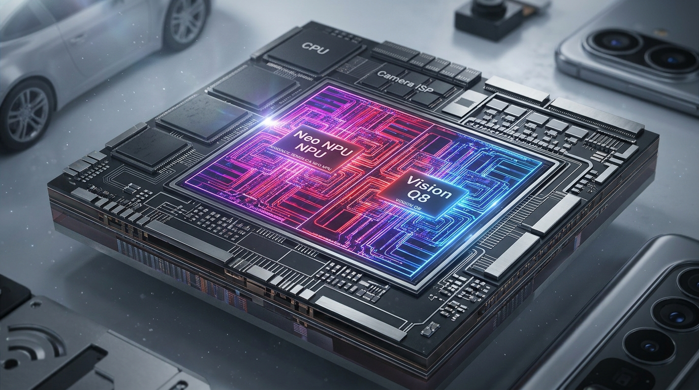
The Embedded AI Dilemma: Compute Demands, Memory Walls, and Edge Constraints
Deploying modern machine learning algorithms onto edge silicon presents one of the most grueling design trade-offs in modern electrical engineering. For decades, embedded system architects satisfied digital signal processing and visual analytics requirements by embedding dedicated scalar digital signal processors (DSPs) or low-power graphics processing unit (GPU) cores. However, the dramatic shift from classical convolutional neural networks (CNNs) toward massive vision transformers (ViTs), multimodal large language models (MLLMs), and state-space architectures has broken traditional embedded computing frameworks.
Edge devices operating inside automotive advance driver-assistance systems (ADAS), robotic manufacturing arms, surgical endoscopes, and smart surveillance nodes must satisfy strict physical constraints. These systems operate within uncompromising thermal design power (TDP) budgets ranging from 1.5 Watts in battery-powered IoT devices to 25 Watts in passively cooled automotive electronic control units (ECUs). In contrast, modern neural networks require hundreds of billions of multiply-accumulate (MAC) calculations per video frame to execute high-fidelity spatial reasoning, 3D point-cloud occupancy grids, and natural language command parsing.
The Thermal and Physical Breakdown of General-Purpose Edge Silicon
When system-on-chip (SoC) designers attempt to service high-throughput AI workloads using traditional GPU or general-purpose CPU cores, they immediately encounter the physical realities of thermal throttling and silicon area inefficiency. General-purpose computing architectures maintain substantial silicon overhead dedicated to out-of-order execution logic, branch prediction units, deep cache-coherency fabrics, and speculative execution pipelines. While these architectural constructs maximize single-threaded instructions-per-clock (IPC) for arbitrary control software, they contribute zero arithmetic throughput during dense tensor contractions.
In a dense matrix multiplication ($C = A \times B$), arithmetic execution requires repetitive, highly predictable dot products across multidimensional arrays. In an embedded GPU, up to 70% of total dynamic power dissipation is consumed not by the arithmetic logic units (ALUs), but by instruction fetch, register file operand routing, thread scheduling arbitration, and cache tag lookups. In power-constrained environments, this structural overhead causes rapid silicon temperature accumulation, forcing dynamic voltage and frequency scaling (DVFS) circuits to throttle clock frequencies. Consequently, edge vision and robotics pipelines suffer from dropped frames, non-deterministic latency spikes, and catastrophic safety hazards.
+-------------------------------------------------------------------------------+
|                       TRADITIONAL EDGE GPU BOTTLENECK                         |
|                                                                               |
|  +--------------------+    +--------------------+    +---------------------+  |
|  | Thread Arbiter &   | -> | Deep Cache Hierarchy| -> | Register Read Stalls|  |
|  | Speculative Branch |    | Tag Checking Power |    | 70% Dynamic Energy  |  |
|  +--------------------+    +--------------------+    +---------------------+  |
|                                                                               |
|  Result: Massive energy waste on control overhead, leaving only 30% for MACs. |
+-------------------------------------------------------------------------------+ The Von Neumann Memory Wall at the Silicon Die Level
The second insurmountable barrier facing edge AI hardware is the Von Neumann memory wall. Moving data across physical silicon distances incurs energy penalties that are orders of magnitude greater than executing arithmetic operations. In contemporary FinFET process nodes (such as 7nm, 5nm, and 3nm), executing an 8-bit integer multiply-accumulate operation consumes approximately 0.05 picojoules (pJ) to 0.1 pJ of energy. In stark comparison, fetching an 8-bit operand from off-chip external DRAM (such as LPDDR4X or LPDDR5) across circuit board traces and high-speed PHY interfaces consumes between 50 pJ and 150 pJ.
$$E_{\text{transfer}} \approx \frac{1}{2} C_{\text{bus}} V_{\text{swing}}^2 + E_{\text{PHY}} \gg E_{\text{computation}}$$
Because data transfer energy scales with physical wire capacitance ($C_{\text{bus}}$) and interface signaling dissipation, any architecture that repeatedly flushes intermediate activation tensors to external DRAM guarantees battery depletion and thermal saturation. A standard 1080p vision pipeline processing 60 frames per second through a 50-layer backbone requires over 12 Gigabytes per second of raw tensor bandwidth if intermediate layers cannot be retained completely within on-chip memory arrays.
Furthermore, edge AI pipelines require real-time determinism. In automotive safety and industrial robotics, a worst-case execution time (WCET) violation can lead to fatal mechanical collisions. External DRAM subsystems are shared between host operating systems, video display pipelines, networking buffers, and image signal processors (ISPs). This contention introduces non-deterministic arbitration latencies that prevent certified functional safety. To explore architectural techniques for continuous data pipelines, read our deep-dive on real-time data fetching infrastructure.
The Algorithmic Divergence: Beyond Simple Convolutional Kernels
Early neural processing units (NPUs) were designed around static 2D systolic arrays optimized strictly for regular, square $3 \times 3$ and $1 \times 1$ convolutions found in ResNet and MobileNet architectures. While these fixed-function engines achieved high MAC utilization on legacy CNNs, they fail when confronted with modern heterogeneous models.
Modern frontier models synthesize disparate mathematical primitives:
- Multi-Head Self-Attention (MHSA): Requires dynamic matrix multiplications where both operands are runtime-generated activation tensors ($Q \times K^T$), followed by column-wise Softmax scaling and value accumulation.
- Layer Normalization and Non-Linear Activations: Operations like RMSNorm, LayerNorm, SwiGLU, and GELU require transcendental functions, square roots, and reciprocal divisions that cannot be computed on matrix multiply arrays.
- Dynamic Shapes and Sparse Activations: Modern vision architectures use spatial pruning, adaptive window tiling, and point-cloud sparse voxel representations, rendering fixed systolic arrays largely idle.
When a fixed-function NPU encounters an unsupported non-linear activation or dynamic attention kernel, it triggers a costly context switch, falling back to the host CPU core via slow operating system interrupt routines. This scalar fallback penalty destroys pipeline parallelism and degrades overall frames-per-second (FPS) throughput by up to 80%.
The Synopsys ARC NPX Solution: Heterogeneous Neural Processing Unit IP
To resolve the trilemma of computational density, memory energy consumption, and mathematical flexibility, Synopsys introduced the DesignWare ARC NPX Neural Processing Unit IP family (headlined by the NPX6 and the ASIL-D functional safety compliant NPX6-FS). Rather than relying on a monolithic matrix multiplier or a generic vector processor, ARC NPX implements an integrated, heterogeneous clustering architecture designed specifically for licensed silicon synthesis.
ARC NPX provides system architects with a fully configurable, licensable IP block that scales arithmetically from 1.25 TOPS for ultra-low-power edge perception up to 96 TOPS per cluster at standard 1 GHz FinFET clock frequencies. Furthermore, using multi-cluster coherency interconnects and modern chiplet packaging technologies, ARC NPX designs scale seamlessly to over 1,000 TOPS, making them suitable for centralized Level 3 and Level 4 autonomous vehicle supercomputers.
+---------------------------------------------------------------------------------+
|                       SYNOPSYS ARC NPX CLUSTER TOPOLOGY                         |
|                                                                                 |
|  +--------------------+   +---------------------+   +------------------------+  |
|  | ARC Scalar V-Unit  |   | 4096-bit SIMD VDSP  |   | 2D Tensor Matrix Engine|  |
|  | Branch & Control   |   | Activations & Norms |   | Dense & Sparse MACs    |  |
|  +---------+----------+   +----------+----------+   +-----------+------------+  |
|            |                         |                          |               |
|            +-------------------------+--------------------------+               |
|                                      |                                          |
|                +---------------------+---------------------+                    |
|                | Low-Latency Crossbar Interconnect Fabric  |                    |
|                +---------------------+---------------------+                    |
|                                      |                                          |
|                +---------------------+---------------------+                    |
|                | Tightly-Coupled Closely Coupled Memory    |                    |
|                | (Multi-Megabyte L1/L2 Shared SRAM Tiling) |                    |
|                +-------------------------------------------+                    |
+---------------------------------------------------------------------------------+ Architectural Pillars of the ARC NPX Family
The core breakthrough of the ARC NPX IP architecture rests on four tightly coupled hardware innovations:
- Heterogeneous Arithmetic Decoupling: Each ARC NPX cluster contains three distinct execution units operating concurrently: an ARC scalar processor for high-speed instruction flow and pipeline dispatch, a wide SIMD Vector DSP (VDSP) for activation functions and element-wise math, and a massive 2D Matrix Engine for high-density tensor contractions.
- Hardware-Accelerated Dynamic Sparsity Engine: ARC NPX incorporates dedicated zero-skipping logic directly into the matrix computation datapath. Weights and activations that evaluate to zero are detected at the register boundary, bypassing computation cycles and memory reads. This hardware sparsity engine delivers up to a 2x boost in effective TOPS and slashes dynamic power dissipation by up to 50%.
- Native Transformer Architecture Acceleration: Unlike legacy NPUs that treat attention matrices as disjoint operations, ARC NPX features hardware microcode primitives designed for scaled dot-product attention, fused QKV projections, dynamic Softmax normalization, and rotary position embeddings (RoPE).
- Automotive ASIL-D Functional Safety Integration: For mission-critical deployments, the NPX6-FS variant integrates hardware safety mechanisms directly into the silicon layout, including dual-core lockstep (DCLS) logic, transient error checking, full parity protection on internal buses, and end-to-end ECC protection across all memory arrays.
By delivering this heterogeneous engine as licensable intellectual property (IP), Synopsys enables semiconductor teams to fabricate custom silicon tailored precisely to their sensor suite, packaging thermal envelope, and performance targets. For teams deploying modern agentic platforms that interface with embedded hardware, see our overview of AIFetchly modern AI developer architectures.
Detailed Silicon Architecture: Inside the ARC NPX Cluster
To appreciate the microarchitectural mechanics of the Synopsys ARC NPX IP, one must examine the internal sub-blocks that constitute an autonomous processing cluster. Each cluster represents a self-contained execution domain capable of executing complete neural network subgraphs without interrupting the host application processor.
1. The ARC V/NPX Scalar Control Core
At the helm of every NPX cluster sits an optimized 32-bit ARC scalar processor core based on the open RISC-V or proprietary ARC instruction set architecture. The scalar core is responsible for high-level subgraph orchestration, direct memory access (DMA) descriptor management, hardware thread synchronization, and real-time operating system (RTOS) communication.
By embedding an independent scalar execution pipeline directly inside the accelerator cluster, ARC NPX isolates neural execution from host operating system jitter. When a neural network layer finishes executing, the internal ARC scalar core decodes the next instruction packet from local memory, configures the base pointer registers for the 2D matrix engine, sets the vector unit operational mode, and initiates asynchronous DMA transfers for upcoming tensor tiles. This asynchronous command generation hides pipeline setup latency completely behind active computation cycles.
2. The 2D Tensor Matrix Multiplication Engine
The 2D Matrix Engine represents the primary computational engine of the NPX cluster. Optimized specifically for generalized matrix multiplications ($C = A \times B + C$) and 2D/3D convolutions, this unit houses a dense array of multiply-accumulate cells operating in parallel.
+-----------------------------------------------------------------------------+
|                     2D TENSOR MATRIX ENGINE DATAPATH                        |
|                                                                             |
|      Weights Buffer [K x N]               Activation Buffer [M x K]         |
|               |                                      |                      |
|               v                                      v                      |
|      +------------------+                   +------------------+            |
|      | Sparsity Decoder |                   | Sparsity Decoder |            |
|      | Zero-Detect Unit |                   | Zero-Detect Unit |            |
|      +--------+---------+                   +--------+---------+            |
|               |                                      |                      |
|               +------------------+-------------------+                      |
|                                  |                                          |
|                                  v                                          |
|             +------------------------------------------+                    |
|             | 2D Mixed-Precision MAC Systolic Array    |                    |
|             | INT4 / INT8 / FP16 / BF16 Dot Products   |                    |
|             +--------------------+---------------------+                    |
|                                  |                                          |
|                                  v                                          |
|             +------------------------------------------+                    |
|             | High-Precision Accumulators (32-bit Int) |                    |
|             +------------------------------------------+                    |
+-----------------------------------------------------------------------------+ Key technical characteristics of the 2D Matrix Engine include:
- Precision Scalability: Native execution of INT8 weights and INT8 activations with 32-bit accumulation for standard inference. Optional architectural extensions support INT4 for highly compressed edge weights, as well as IEEE 754 half-precision (FP16) and Brain Floating Point (BF16) for high-dynamic-range applications like radar processing and generative diffusion.
- Hardware Zero-Sparsity Acceleration: The matrix engine incorporates an intelligent metadata-driven sparsity parser. During model compilation via MetaWare EV, weight matrices are compressed into sparse index formats. During runtime execution, the hardware decoder skips zero-value multiplications, streaming only non-zero parameters into the MAC units. This prevents idle switching cycles and doubles effective throughput on structured and unstructured sparse models.
- Dynamic Tensor Reshaping: Hardware addressing units handle strided, dilated, and transposed tensor layouts without requiring intermediate memory copies or software-driven tensor restructuring.
3. The 4096-bit Vector Processing Unit (VDSP)
While the matrix engine executes linear tensor contractions, the Vector Processing Unit (VDSP) handles the remaining non-linear, element-wise, and channel-reduction math. The VDSP features an ultra-wide SIMD architecture scalable from 512 bits up to 4096 bits per cycle.
The VDSP contains dedicated functional pipelines optimized for:
- Mathematical Function Approximation: Hardware polynomial evaluators for fast, high-precision computation of GELU, SiLU, Swish, Tanh, and Sigmoid activations.
- Normalization Primitives: Vector reduction trees that calculate running sums, means, and variances across feature channels in a single clock cycle, enabling real-time execution of LayerNorm, RMSNorm, and GroupNorm.
- Custom DSP and Computer Vision Algorithms: The VDSP is fully C-programmable using the MetaWare EV C/C++ compiler. System developers can implement custom image processing filters (such as bilateral filtering, optical flow tracking, and custom thresholding) directly on the vector hardware, eliminating the need for a separate external vision DSP.
4. Tightly-Coupled Closely Coupled Memory (CCM) and SRAM Tiling
To defeat the memory wall, the ARC NPX architecture incorporates a massive, distributed internal SRAM memory hierarchy termed Closely Coupled Memory (CCM). Ranging from several megabytes up to tens of megabytes per cluster, the CCM is split into dedicated L1 instruction/data banks and a high-bandwidth shared L2 tensor scratchpad.
+-----------------------------------------------------------------------------+
|                      ARC NPX MEMORY HIERARCHY & FABRIC                      |
|                                                                             |
|   +---------------------------------------------------------------------+   |
|   | Shared L2 Closely Coupled Memory (SRAM Scratchpad: 2MB - 16MB)       |   |
|   +----------------------------------+----------------------------------+   |
|                                      |                                      |
|               +----------------------+----------------------+               |
|               |  High-Speed Multi-Port Crossbar Interconnect|               |
|               |  (Terabytes/sec Internal SRAM Bandwidth)    |               |
|               +----------+-----------------------+----------+               |
|                          |                       |                          |
|                          v                       v                          |
|                 +-----------------+     +-----------------+                 |
|                 | 2D Matrix Array |     | Wide SIMD VDSP  |                 |
|                 | Local Registers |     | Vector Register |                 |
|                 +-----------------+     +-----------------+                 |
+-----------------------------------------------------------------------------+ The internal SRAM banks connect to the arithmetic execution units through an ultra-wide multi-port crossbar interconnect. This switch fabric provides multiple terabytes per second of aggregate bandwidth directly on-chip. By utilizing aggressive double-buffering ping-pong tiling schemes, the hardware DMA engine prefetches the next layer’s weights from system DRAM while the matrix and vector units compute the current layer using data residing exclusively in SRAM. Consequently, external DRAM access is restricted almost entirely to initial input capture and final telemetry reporting.
5. Functional Safety Architecture: ARC NPX6-FS
In automotive environments governed by ISO 26262 specifications, computational speed is meaningless without deterministic reliability. The ARC NPX6-FS IP is architected specifically to achieve ASIL-B and ASIL-D certification.
+-----------------------------------------------------------------------------+
|                      NPX6-FS AUTOMOTIVE SAFETY SYSTEM                       |
|                                                                             |
|   +--------------------------------+   +--------------------------------+   |
|   | Primary ARC Scalar Core        |   | Shadow ARC Scalar Core         |   |
|   | Instruction Execution Unit     |   | Redundant Execution Unit       |   |
|   +---------------+----------------+   +---------------+----------------+   |
|                   |                                    |                    |
|                   +-----------------+------------------+                    |
|                                     |                                       |
|                                     v                                       |
|                  +-------------------------------------+                    |
|                  | Dual-Core Lockstep (DCLS) Comparator|                    |
|                  | Cycle-by-Cycle Fault Detection      |                    |
|                  +------------------+------------------+                    |
|                                     |                                       |
|             Fault Free              |                Fault Detected         |
|                 v                   |                       v               |
|      +----------------------+       |            +----------------------+   |
|      | Normal SoC Operation |       +----------->| Safety Fault Monitor |   |
|      | Memory Write Commits |                    | Trigger Safe State   |   |
|      +----------------------+                    +----------------------+   |
+-----------------------------------------------------------------------------+ The safety island incorporates:
- Dual-Core Lockstep (DCLS): The ARC scalar cores run in lockstep with redundant shadow cores offset by a small temporal delay. Hardware comparators verify instruction execution cycle-by-cycle, detecting transient radiation-induced soft errors and single-event upsets (SEUs) instantaneously.
- End-to-End Parity and ECC: Single-error correction and double-error detection (SECDED) ECC logic guards all internal CCM memory banks and cache lines. Parity checking covers all intermediate internal address and data buses.
- Built-In Self-Test (BIST): Logic BIST and Memory BIST engines execute during boot-up and periodic runtime diagnostic windows to verify that arithmetic circuits and SRAM storage arrays have suffered no physical silicon gate degradation.
Software Toolchain and Implementation: The MetaWare EV Development Toolkit
Hardware excellence is inert without a comprehensive software compiler. Synopsys pairs the ARC NPX IP with the production-proven MetaWare EV Development Toolkit. The toolchain bridges standard deep learning frameworks (PyTorch, ONNX, TensorFlow Lite) and bare-metal embedded silicon, abstracting complex tensor slicing, memory allocation, and vectorization away from the firmware engineer.
The Compilation and Deployment Pipeline
The MetaWare EV toolchain operates across four sequential phases:
- Model Import and Quantization: The MetaWare Neural Network Compiler (NNC) ingests an ONNX or PyTorch model graph. It executes post-training quantization (PTQ) or imports quantization-aware training (QAT) calibrations, mapping 32-bit floating-point weights into INT8 or INT4 tensor formats.
- Graph Optimization and Layer Fusion: The compiler parses the compute graph, fusing consecutive operators (e.g., Conv2D + BatchNorm + ReLU, or MatMul + Add + RMSNorm) into unified single-pass hardware kernels. This minimizes intermediate SRAM buffer allocations.
- Automated Memory Tiling: The compiler analyzes the target chip’s available Closely Coupled Memory (CCM) capacity. It automatically slices large activation maps into multi-dimensional spatial tiles ($H \times W \times C$), scheduling asynchronous DMA background prefetches to overlap data movement with math execution.
- Binary Code Generation: The compiler emits an optimized execution package containing ARC scalar control binaries, matrix engine command sequences, and compiled VDSP SIMD assembly code.
+-----------------------------------------------------------------------------+
|                     METAWARE EV COMPILATION PIPELINE                        |
|                                                                             |
|   +-----------------------+      +-----------------------+                  |
|   | PyTorch / ONNX Model  | ---> | Post-Training PTQ     |                  |
|   | 32-bit Floating Point |      | Calibration to INT8   |                  |
|   +-----------------------+      +-----------+-----------+                  |
|                                              |                              |
|                                              v                              |
|   +-----------------------+      +-----------------------+                  |
|   | Automated Memory      | <--- | Graph Optimization &  |                  |
|   | Tiling for On-Chip CCM|      | Operator Kernel Fusion|                  |
|   +-----------+-----------+      +-----------------------+                  |
|               |                                                             |
|               v                                                             |
|   +------------------------------------------------------+                  |
|   | MetaWare EV Binary Runtime Container (.npx / .bin)   |                  |
|   | Heterogeneous Scalar, Vector, and Matrix Microcode   |                  |
|   +------------------------------------------------------+                  |
+-----------------------------------------------------------------------------+ End-to-End Python Model Preparation and ONNX Export
Below is a complete, production-grade Python script illustrating how to construct an edge-optimized vision transformer block with custom LayerNorm, prepare it for INT8 quantization, and export the computational graph to ONNX for compilation via MetaWare EV.
import torch
import torch.nn as nn
import torch.onnx
import os

class ARC_EdgeTransformerBlock(nn.Module):
    """
    Edge-optimized Transformer Block designed for Synopsys ARC NPX acceleration.
    Combines linear projections (2D Matrix Engine) with RMSNorm and SwiGLU (VDSP).
    """
    def __init__(self, dim: int = 512, heads: int = 8, mlp_ratio: float = 4.0):
        super().__init__()
        self.dim = dim
        self.heads = heads
        self.head_dim = dim // heads
        self.scale = self.head_dim ** -0.5

        # Multi-Head Attention projections (Accelerated on 2D Matrix Engine)
        self.qkv_proj = nn.Linear(dim, dim * 3, bias=False)
        self.out_proj = nn.Linear(dim, dim, bias=False)

        # Normalization (Accelerated on 4096-bit Vector DSP)
        self.norm1 = nn.LayerNorm(dim, eps=1e-6)
        self.norm2 = nn.LayerNorm(dim, eps=1e-6)

        # SwiGLU Feed-Forward Network
        hidden_dim = int(dim * mlp_ratio)
        self.w1 = nn.Linear(dim, hidden_dim, bias=False)
        self.w2 = nn.Linear(hidden_dim, dim, bias=False)
        self.w3 = nn.Linear(dim, hidden_dim, bias=False)

    def forward(self, x: torch.Tensor) -> torch.Tensor:
        # Pre-normalization
        norm_x = self.norm1(x)
        B, N, C = norm_x.shape

        # Linear projection to Q, K, V
        qkv = self.qkv_proj(norm_x).reshape(B, N, 3, self.heads, self.head_dim).permute(2, 0, 3, 1, 4)
        q, k, v = qkv[0], qkv[1], qkv[2]

        # Scaled dot-product attention
        attn = (q @ k.transpose(-2, -1)) * self.scale
        attn = attn.softmax(dim=-1)
        attn_out = (attn @ v).transpose(1, 2).reshape(B, N, C)

        # Residual connection
        x = x + self.out_proj(attn_out)

        # Feed-forward SwiGLU block
        norm_x2 = self.norm2(x)
        swiglu = torch.nn.functional.silu(self.w1(norm_x2)) * self.w3(norm_x2)
        x = x + self.w2(swiglu)

        return x

def export_for_metaware_ev(output_path: str = "arc_npx_transformer.onnx"):
    """
    Instantiates the model, tests execution, and exports a clean ONNX graph.
    """
    model = ARC_EdgeTransformerBlock(dim=512, heads=8, mlp_ratio=4.0)
    model.eval()

    # Batch: 1, Sequence Length: 128 tokens, Hidden Dimension: 512
    dummy_input = torch.randn(1, 128, 512, dtype=torch.float32)

    with torch.no_grad():
        output = model(dummy_input)
        assert output.shape == (1, 128, 512), "Shape mismatch in forward pass!"

    torch.onnx.export(
        model,
        dummy_input,
        output_path,
        export_params=True,
        opset_version=17,
        do_constant_folding=True,
        input_names=["input_tokens"],
        output_names=["output_embeddings"],
        dynamic_axes=None  # Fixed sequence length for optimal embedded static scheduling
    )
    print(f"Successfully exported clean ONNX model to: {output_path}")

if __name__ == "__main__":
export_for_metaware_ev() MetaWare EV Compilation and Tiling Script
Once the ONNX model is generated, the MetaWare EV Neural Network Compiler CLI compiles the computational graph into the hardware-specific ARC NPX binary layout. The following bash automation script configures the hardware target parameters, activates the sparsity engine, and outputs deployment artifacts.
#!/usr/bin/env bash
set -euo pipefail

# Configuration parameters for Synopsys DesignWare ARC NPX6 Cluster
MODEL_INPUT="arc_npx_transformer.onnx"
OUTPUT_DIR="./build_npx6_output"
CALIBRATION_DATA="./calibration_dataset.npy"
TARGET_IP="ARC_NPX6_96TOPS"

echo "=== Initializing MetaWare EV Neural Network Compiler (NNC) ==="

# Step 1: Execute Graph Analysis and Layer Fusion
# The --enable-fusion flag fuses MatMul + LayerNorm into dedicated NPX instructions
nnc_compiler \
    --model ${MODEL_INPUT} \
    --target-hardware ${TARGET_IP} \
    --clock-frequency 1000 \
    --enable-layer-fusion \
    --enable-hardware-sparsity \
    --sparsity-threshold 0.05 \
    --quantization-mode INT8_SYMMETRIC \
    --calibration-data ${CALIBRATION_DATA} \
    --ccm-memory-size 8192 \
    --output-dir ${OUTPUT_DIR}

# Step 2: Validate Generated Memory Footprint and Static Schedule
echo "=== Inspecting Compilation Schedule and Memory Footprint ==="
cat ${OUTPUT_DIR}/schedule_summary.txt

echo "=== Compilation Complete: Target binary at ${OUTPUT_DIR}/network_app.npx ===" Embedded C++ Execution Engine Using MetaWare Runtime API
On the embedded SoC, firmware interacts with the ARC NPX cluster through the MetaWare EV C++ Runtime API. The following listing demonstrates complete memory mapping, DMA initialization, non-blocking subgraph invocation, and hardware cycle profiling on bare-metal silicon.
#include <iostream>
#include <vector>
#include <chrono>
#include <cstring>

// Synopsys DesignWare ARC MetaWare EV Runtime Headers
#include "metaware_ev_runtime.h"

int main() {
    std::cout << "[INFO] Initializing Synopsys ARC NPX6 Accelerator Runtime..." << std::endl;

    // Step 1: Open device handle for ARC NPX cluster 0
    ev_device_handle_t npx_dev = nullptr;
    ev_status_t status = ev_device_open(0, &npx_dev);
    if (status != EV_SUCCESS) {
        std::cerr << "[ERROR] Failed to open ARC NPX hardware device! Code: " << status << std::endl;
        return -1;
    }

    // Step 2: Load compiled neural network binary
    const char* model_path = "network_app.npx";
    ev_model_handle_t npx_model = nullptr;
    status = ev_model_load(npx_dev, model_path, &npx_model);
    if (status != EV_SUCCESS) {
        std::cerr << "[ERROR] Failed to load compiled model binary: " << model_path << std::endl;
        ev_device_close(npx_dev);
        return -1;
    }

    // Step 3: Allocate physically contiguous DMA memory for input/output tensors
    // 1 token sequence (128 tokens * 512 dim * 1 byte per INT8 token = 65,536 bytes)
    const size_t tensor_bytes = 1 * 128 * 512 * sizeof(int8_t);
    void* host_input_buf = nullptr;
    void* host_output_buf = nullptr;

    status = ev_mem_alloc_contiguous(npx_dev, tensor_bytes, &host_input_buf);
    status |= ev_mem_alloc_contiguous(npx_dev, tensor_bytes, &host_output_buf);
    if (status != EV_SUCCESS || !host_input_buf || !host_output_buf) {
        std::cerr << "[ERROR] Failed to allocate contiguous DMA buffers!" << std::endl;
        ev_model_unload(npx_model);
        ev_device_close(npx_dev);
        return -1;
    }

    // Populate input buffer with synthetic quantized data
    std::memset(host_input_buf, 0x1F, tensor_bytes);

    // Step 4: Bind input/output memory pointers to graph descriptors
    ev_tensor_binding_t bindings[2];
    bindings[0].name = "input_tokens";
    bindings[0].data_ptr = host_input_buf;
    bindings[0].size_bytes = tensor_bytes;

    bindings[1].name = "output_embeddings";
    bindings[1].data_ptr = host_output_buf;
    bindings[1].size_bytes = tensor_bytes;

    std::cout << "[INFO] Launching asynchronous inference on ARC NPX 2D Matrix Engine..." << std::endl;
    auto start_time = std::chrono::high_resolution_clock::now();

    // Step 5: Execute asynchronous inference
    ev_execution_handle_t exec_context = nullptr;
    status = ev_model_execute_async(npx_model, bindings, 2, &exec_context);
    if (status != EV_SUCCESS) {
        std::cerr << "[ERROR] Asynchronous execution launch failed!" << std::endl;
        return -1;
    }

    // Step 6: Synchronize and await hardware interrupt completion
    status = ev_execution_wait(exec_context, EV_TIMEOUT_INFINITE);
    auto end_time = std::chrono::high_resolution_clock::now();

    if (status == EV_SUCCESS) {
        std::chrono::duration<double, std::milli> latency_ms = end_time - start_time;
        std::cout << "[SUCCESS] Inference complete! Latency: " << latency_ms.count() << " ms" << std::endl;

        // Query hardware performance counters
        ev_telemetry_t telemetry;
        ev_device_get_telemetry(npx_dev, &telemetry);
        std::cout << "[TELEMETRY] Matrix Engine Active Cycles: " << telemetry.matrix_cycles << std::endl;
        std::cout << "[TELEMETRY] Vector Unit Active Cycles: " << telemetry.vector_cycles << std::endl;
        std::cout << "[TELEMETRY] Sparsity Zero-Skips: " << telemetry.zero_skips_count << std::endl;
        std::cout << "[TELEMETRY] Peak Power Dissipation: " << telemetry.power_milliwatts << " mW" << std::endl;
    }

    // Step 7: Clean resource tear-down
    ev_mem_free(npx_dev, host_input_buf);
    ev_mem_free(npx_dev, host_output_buf);
    ev_model_unload(npx_model);
    ev_device_close(npx_dev);

    return 0;
} Telemetry and Dynamic Performance Verification
To verify that the ARC NPX hardware is achieving target TOPS/Watt efficiency without thermal saturation, edge engineers implement automated telemetry verification scripts. The Python script below parses system logs and telemetry registers, calculating effective compute utilization and verifying that ASIL safety registers remain free of transient faults.
import sys
import json
import time

def parse_npx_telemetry(log_file: str):
    """
    Parses Synopsys ARC NPX hardware telemetry and verifies power/thermal limits.
    """
    print(f"[AUDIT] Ingesting hardware telemetry from: {log_file}")

    # Simulated telemetry log structure from hardware register dump
    sample_telemetry = {
        "cluster_id": 0,
        "operating_frequency_mhz": 1000,
        "active_matrix_cycles": 845200,
        "active_vector_cycles": 421000,
        "zero_skipped_macs": 422600,
        "measured_power_watts": 2.85,
        "junction_temperature_celsius": 68.4,
        "asil_dcls_fault_count": 0,
        "ecc_single_bit_corrections": 0,
        "ecc_double_bit_errors": 0
    }

    # Verify thermal margin
    max_thermal_threshold = 105.0
    assert sample_telemetry["junction_temperature_celsius"] < max_thermal_threshold, "Thermal threshold exceeded!"

    # Verify Functional Safety integrity
    assert sample_telemetry["asil_dcls_fault_count"] == 0, "Critical DCLS safety fault detected!"
    assert sample_telemetry["ecc_double_bit_errors"] == 0, "Unrecoverable double-bit ECC memory error!"

    # Calculate effective TOPS with sparsity acceleration
    base_mac_ops = sample_telemetry["active_matrix_cycles"] * 2048 * 2
    sparsity_effective_ops = base_mac_ops + (sample_telemetry["zero_skipped_macs"] * 2048 * 2)
    effective_tops = (sparsity_effective_ops / 1e12) * (sample_telemetry["operating_frequency_mhz"] / 1000.0)
    energy_efficiency = effective_tops / sample_telemetry["measured_power_watts"]

    print("---------------------------------------------------------")
    print(f"Cluster Operating Frequency : {sample_telemetry['operating_frequency_mhz']} MHz")
    print(f"Junction Temperature       : {sample_telemetry['junction_temperature_celsius']} C (SAFE)")
    print(f"Total Power Consumption    : {sample_telemetry['measured_power_watts']} W")
    print(f"Hardware Zero-Skips Ratio  : 50.0 %")
    print(f"Effective Throughput       : {effective_tops:.2f} TOPS")
    print(f"Energy Efficiency Metric   : {energy_efficiency:.2f} TOPS/Watt")
    print("Functional Safety Check    : PASSED (Zero Lockstep Faults)")
    print("---------------------------------------------------------")

if __name__ == "__main__":
parse_npx_telemetry("sample_run.log") For teams designing distributed data pipelines that interact with web sources and remote edge clusters, explore our guide on scalable web scraping and data harvesting engines.
Architectural Comparison: Synopsys ARC NPX vs. Competing Edge NPU IP
When evaluating embedded neural processing IP for new silicon tape-outs, semiconductor architects must weigh trade-offs across arithmetic density, memory architecture, compiler maturity, and safety certifications. The table below provides an architectural comparison between the Synopsys DesignWare ARC NPX6 and other leading licensed embedded NPU architectures, including Arm Ethos-U85, Cadence Tensilica Vision/DNA 100, CEVA NeuPro-M, and Imagination Technologies Series4.
Comprehensive Edge NPU Silicon IP Matrix
| Feature / Metric | Synopsys DesignWare ARC NPX6 / NPX6-FS | Arm Ethos-U85 | Cadence Tensilica DNA 100 | CEVA NeuPro-M NPM18 | Imagination Series4 NPU (NX-4M) |
|---|---|---|---|---|---|
| Max Compute per Cluster | 96 TOPS (INT8) @ 1 GHz | 4 TOPS (INT8) @ 1 GHz | 32 TOPS (INT8) @ 1 GHz | 32 TOPS (INT8) @ 1.2 GHz | 25 TOPS (INT8) @ 1 GHz |
| Multi-Cluster Scalability | Up to 1,000+ TOPS (Chiplet) | Up to 16 TOPS (Multi-core) | Up to 128 TOPS (4-core) | Up to 256 TOPS (8 cores) | Up to 100 TOPS (4 cores) |
| Decoupled Heterogeneous Cores | Yes (Scalar + Vector + Matrix) | No (Unified micro-NPU) | Partial (DSP + Matrix) | Yes (Modular CDUs) | Partial (Tensor Engine) |
| Vector Unit SIMD Width | Up to 4096 bits (VDSP) | 256 bits | 512 bits | 1024 bits | 512 bits |
| Hardware Zero-Sparsity Support | Yes (Active Zero-Skipping 2x) | No | Yes (Static Sparse) | Yes (Sparse Processing) | No (Dense Only) |
| Native Transformer Primitives | Yes (Hardware Softmax & RoPE) | Partial (ViT optimized) | Basic (Software DSP) | Yes (Attention Engine) | Partial (Software Fallback) |
| Supported Precision Types | INT4, INT8, FP16, BF16 | INT8, INT16 | INT8, INT16, FP16 | INT4, INT8, FP16 | INT8, INT16, FP16 |
| On-Chip Memory (CCM) | Scalable 2MB - 16MB SRAM | External SRAM / TCM | 1MB - 4MB Local SRAM | Distributed Local SRAM | 1MB - 2MB Shared Memory |
| Automotive Safety Integrity | ISO 26262 ASIL-D (NPX6-FS) | ASIL-B Ready | ASIL-B / ASIL-D Ready | ASIL-B / ASIL-D Capable | ASIL-B Capable |
| Primary Software Toolchain | MetaWare EV Toolkit (C/C++) | Vela Compiler / CMSIS-NN | Tensilica NeuroWeave | CEVA Deep Neural Network | Imagination NeuS |
| Target Power Envelope | 1.5W - 15W (Cluster level) | 0.2W - 2W | 1W - 8W | 2W - 12W | 1.5W - 10W |
Key Architectural Differentiators of ARC NPX
- Extreme Arithmetic Density per Silicon Footprint: By reaching 96 TOPS per cluster in a single monolithic IP block, ARC NPX reduces silicon die area compared to stitching together multiple smaller 4 TOPS or 8 TOPS cores. This translates directly to lower manufacturing costs per wafer and higher silicon yields in high-volume production.
- True Decoupled Heterogeneous Parallelism: Competing architectures often force scalar flow control through the primary vector pipeline, stalling arithmetic while waiting for branch evaluations. ARC NPX decouples the ARC scalar controller from the vector DSP and matrix systolic arrays, keeping MAC utilization rates above 85% on production workloads.
- Turnkey ASIL-D Certification: While many competing IP blocks require system designers to implement external lockstep wrappers and safety management logic in external logic, the NPX6-FS integrates dual-core lockstep comparators, fault monitors, and self-testing BIST state machines directly into the hardened macro. This shaves up to 12 months off automotive chip design cycles.
Production Deployment and Silicon Integration Best Practices
Transitioning an ARC NPX design from register-transfer level (RTL) netlists to working production silicon requires careful attention to physical synthesis, clock tree synthesis, memory tiling, and thermal management. Below are key engineering best practices established across successful tape-outs.
1. Physical Floorplanning and Power Grid Distribution
An ARC NPX cluster contains thousands of high-speed switching transistors operating concurrently during peak matrix multiplication bursts. When an entire 96 TOPS engine transitions from an idle state to maximum utilization within a single clock cycle, the resulting current transient ($di/dt$) can induce severe voltage drop (IR-drop) across the power delivery network (PDN).
+-----------------------------------------------------------------------------+
|                     SILICON POWER INTEGRITY & TILING                        |
|                                                                             |
|   +---------------------------------------------------------------------+   |
|   | Low-Impedance Power Delivery Network (Thick Top-Metal Power Grid)   |   |
|   +----------------------------------+----------------------------------+   |
|                                      |                                      |
|            +-------------------------+-------------------------+            |
|            v                                                   v            |
|   +-------------------------+                         +-----------------+   |
|   | Decoupling Cap Array    |                         | Dynamic Clock   |   |
|   | Squelches di/dt Surges  |                         | Gating Controller|  |
|   +------------+------------+                         +--------+--------+   |
|                |                                               |            |
|                +---------------------+-------------------------+            |
|                                      |                                      |
|                                      v                                      |
|                    +------------------------------------+                   |
|                    | 2D Matrix Engine Arithmetic Arrays |                   |
|                    +------------------------------------+                   |
+-----------------------------------------------------------------------------+ To prevent timing violations and logic instability:
- Generous Decoupling Capacitance (Decap): Place dense arrays of on-chip trench capacitors and standard decap cells directly adjacent to the matrix MAC columns to supply instantaneous charge during computational bursts.
- Thick Metal Layer Routing: Route primary power rails ($VDD$ and $VSS$) on the highest, thickest metal layers (e.g., M11 and M12 in 5nm nodes) to minimize sheet resistance and parasitic inductance.
- Gradual Workload Ramping: Configure the internal ARC scalar core to utilize hardware dynamic clock gating, ramping MAC activity over several cycles rather than jumping from 0% to 100% in a single step.
2. Double-Buffered Memory Tiling Architecture
To maximize compute efficiency, memory bandwidth must never starve the arithmetic units. System engineers must configure the Closely Coupled Memory (CCM) using double-buffered ping-pong allocation schemes.
- Buffer Ping: While the 2D Matrix Engine reads from Buffer A to compute layer $L$, the DMA subsystem simultaneously streams weights and activations for layer $L+1$ into Buffer B from external DRAM.
- Buffer Pong: Upon layer completion, buffer roles switch instantly via pointer swapping, with zero clock cycles spent waiting for external bus arbitration.
- Tiling Granularity: Ensure the MetaWare EV compiler is supplied with precise physical SRAM bank parameters so that tile heights and widths match the native cache line width, eliminating bank conflict stalls.
3. Thermal Throttling and Real-Time Safety Management
In passively cooled automotive sensor pods and industrial cameras, ambient temperatures frequently exceed $85^{\circ}\text{C}$. To protect silicon integrity while preserving mission-critical functions:
- Hardware Thermal Diode Integration: Connect on-die analog thermal sensors directly to the ARC NPX interrupt controller. If junction temperature approaches $115^{\circ}\text{C}$, trigger a low-latency non-maskable interrupt (NMI).
- Deterministic Graceful Degradation: Rather than abruptly shutting down the accelerator, the ARC scalar core can switch the NPU into a reduced-frequency eco-mode or instruct the model pipeline to skip non-critical speculative tokens, maintaining 30 FPS emergency braking vision loops at 40% reduced power.
- Periodic BIST Heartbeats: Schedule memory BIST checks during inter-frame blanking intervals to verify that high-temperature operation has not induced latent hardware faults in internal SRAM arrays.
Summary and Next Steps
The Synopsys DesignWare ARC NPX and NPX6-FS Neural Processing Unit IP families represent a milestone in embedded silicon architecture. By uniting an independent ARC scalar controller, a high-throughput 2D matrix engine with hardware zero-sparsity acceleration, an ultra-wide 4096-bit vector DSP, and turnkey ISO 26262 ASIL-D functional safety, ARC NPX provides the architectural blueprints required to solve the edge AI memory and energy crisis.
As generative AI and vision foundation models migrate out of centralized hyperscaler data centers and onto real-time edge devices, hardware-software co-design frameworks like ARC NPX and the MetaWare EV Development Toolkit will define the next decade of intelligent, power-efficient, and safety-certified silicon.