SpiNNaker 2 Guide: 10-Million Core Neuromorphic AI
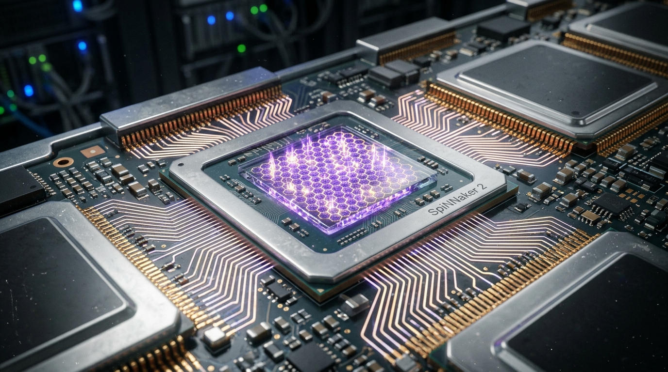
The Problem: The Clocked Computing Crisis and the Communication Wall in Event-Driven AI
Modern computing systems are bound by a foundational dogma established over seven decades ago: synchronous, clock-driven execution over a centralized shared memory hierarchy. In high-performance enterprise systems such as the AI Fetchly high-throughput inference engine, traditional graphics processing units (GPUs) and server CPUs rely on global clock frequencies operating in gigahertz synchrony to process dense, uniform arrays of numbers.
However, the physical world—along with biological neural computation—does not operate on a uniform global clock. Natural sensory inputs from event-based sensors (such as neuromorphic Dynamic Vision Sensors, audio cochlea microphones, and tactile sensors) generate continuous, sparse streams of asynchronous events. Forcing sparse, event-driven temporal signals through dense, clocked digital processors creates massive systemic inefficiencies.
Clocked GPU Dense Processing vs. SpiNNaker 2 Asynchronous Event Routing:
┌─────────────────────────────────────────────────────────────────────────┐
│ Synchronous Clocked GPU / NPU Architecture:                             │
│ ┌─────────────────────────────────────────────────────────────────────┐ │
│ │ Global Clock Grid ──► Dense Tensor Frames ──► High Idle Leakage     │ │
│ │ ❌ 95% of data is static/empty; GPU processes redundant pixels     │ │
│ │ ❌ High-power memory bus saturation; millisecond buffer latencies   │ │
│ │ ❌ Centralized memory locks bottleneck large-scale neural routing   │ │
│ └─────────────────────────────────────────────────────────────────────┘ │
└─────────────────────────────────────────────────────────────────────────┘
                                     ▼
┌─────────────────────────────────────────────────────────────────────────┐
│ SpiNNaker 2 Neuromorphic Event-Driven Architecture:                     │
│ ┌─────────────────────────────────────────────────────────────────────┐ │
│ │ 152 Energy-Optimized ARM Cores per Chip (Scaling to 10 Million)     │ │
│ │ ✅ True Event-Driven: Cores compute ONLY when a spike packet arrives │ │
│ │ ✅ Microsecond Asynchronous Multicast Hardware Routing Mesh          │ │
│ │ ✅ Hybrid Support for Spiking Neural Networks (SNN) & Standard ANNs │ │
│ └─────────────────────────────────────────────────────────────────────┘ │
└─────────────────────────────────────────────────────────────────────────┘ The Inefficiency of Clock-Driven Digital Accelerators on Event-Driven Data
In traditional computer vision pipelines, camera sensors capture static 2D frames at fixed intervals (e.g., 30 or 60 frames per second). Each frame is transmitted as a dense matrix of millions of pixels, regardless of whether anything in the scene has moved:
- Redundant Computational Waste: When an enterprise surveillance or autonomous drone system processes a static scene, the GPU continuously computes billions of floating-point convolutions on unchanged pixels, burning hundreds of watts of power.
- Temporal Aliasing: If a high-speed anomaly occurs between discrete camera frames, conventional video sensors miss the event entirely. Conversely, neuromorphic Dynamic Vision Sensors (DVS) emit individual pixel events (spikes) asynchronously with microsecond temporal resolution only when local brightness changes.
- The GPU Frame-Buffering Penalty: When event-based sensor streams are fed into conventional GPUs, the software must artificially accumulate asynchronous events into artificial dense frame bins over 10 to 50 milliseconds. This frame accumulation destroys the temporal precision of the spikes and re-introduces the latency bottlenecks of clocked computing.
When scaling data extraction across thousands of continuous industrial sensor nodes, such as distributed AI data extraction pipelines monitoring factory equipment, synchronous cloud processing wastes megawatts of electrical power processing static, non-informative telemetry.
The Communication Bottleneck in Large-Scale Neural Simulations
When neuroscientists and computer engineers attempt to simulate biological brains or scale massive graph-structured neural networks containing billions of synapses, they run into the communication wall:
- The Shared-Memory Lockout: Traditional high-performance computing (HPC) clusters rely on shared-memory multi-threading or message-passing interfaces (MPI) across InfiniBand networks. In a biological brain, each neuron connects to thousands of downstream neurons via branching axonal arborizations. Simulating this high-fanout connectivity on conventional clusters requires routing millions of point-to-point network packets, causing severe switch buffer congestion and memory locks.
- Synchronization Barriers: In synchronous simulators, every simulated neuron must wait for the slowest processor to finish its timestep before advancing to the next cycle. This global barrier synchronization creates pipeline idle time and limits physical scalability.
Why Monolithic GPUs Fail on Sparse, Event-Based Edge Robotics
In autonomous robotics, closed-loop latency is the difference between safe navigation and catastrophic collision. Edge robots require sub-millisecond reaction times across motor control, balance reflexes, and obstacle avoidance:
- Thermal Saturation: Monolithic GPUs consume between 30W and 70W at the edge, requiring heavy cooling fans and rapidly draining robot batteries.
- Lack of Adaptive Power Scaling: Even when a robot is stationary and sensory inputs are quiet, a GPU continues to draw high baseline idle power. True edge autonomy demands processors that draw power strictly proportional to environmental activity—consuming milliwatts when idle and bursting power only when rapid events occur.
The Solution: SpiNNaker 2 and the Asynchronous Event-Based Computing Paradigm
To solve the communication wall and eliminate clocked computing waste, the SpiNNaker 2 project was developed through a prestigious international collaboration between the Chair of Highly-Parallel VLSI Systems and Neuromorphic Circuits at Technische Universität Dresden (TU Dresden), led by Prof. Christian Mayr, and the University of Manchester, led by Prof. Steve Furber (the legendary co-designer of the original ARM 32-bit microprocessor).
SpiNNaker 2 System Hierarchy: From Single Core to 10-Million Core Supercomputer
┌─────────────────────────────────────────────────────────────────────────┐
│ Processing Element (PE): ARM Cortex-M4F + 128KB SRAM + Math Accelerators│
│ └──────────────────────────────────┬──────────────────────────────────┘ │
│                                    │ x152 Cores                         │
│                     ┌──────────────▼─────────────┐                      │
│                     │ SpiNNaker 2 SoC (7nm/28nm) │                      │
│                     │ 152 PEs + Multicast Router │                      │
│                     └──────────────┬─────────────┘                      │
│                                    │ x48 Chips                          │
│                     ┌──────────────▼─────────────┐                      │
│                     │ SpiNNaker 2 Board (PCB)    │                      │
│                     │ 7,296 ARM Cores per Board  │                      │
│                     └──────────────┬─────────────┘                      │
│                                    │ Multi-Rack 3D Torus Interconnect   │
│ ┌──────────────────────────────────▼──────────────────────────────────┐ │
│ │ SpiNNcloud Datacenter Supercomputer:                                │ │
│ │ ✅ 10 Million ARM Cores | 1.2 Terabytes of Fast Distributed SRAM     │ │
│ │ ✅ Microsecond Spike Multicast Across Massive Biological Scales      │ │
│ │ ✅ Hybrid Support for Spiking Neural Networks (SNN) & Dense ANNs     │ │
│ └─────────────────────────────────────────────────────────────────────┘ │
└─────────────────────────────────────────────────────────────────────────┘ SpiNNaker 2 (Spiking Neural Network Architecture 2) is a massively parallel digital neuromorphic computing platform that bridges the gap between biological brain simulation and commercial edge machine learning. Packing 152 energy-optimized ARM Cortex-M4F cores on each chip and scaling to 10 million cores in the commercial SpiNNcloud supercomputer, SpiNNaker 2 delivers event-driven execution with microsecond packet routing and exceptional energy efficiency.
From Biological Brains to Silicon: The SpiNNaker 2 Philosophy
The architectural design of SpiNNaker 2 is guided by three biological principles:
- Event-Driven Computation: Neurons in biological brains do not fire on a periodic clock; they remain quiet until incoming electrical potentials cross a threshold. In SpiNNaker 2, processor cores remain in deep low-power sleep states, waking up only when an asynchronous packet arrives, processing the event in microseconds, and immediately returning to sleep.
- Massive Parallelism with Distributed Memory: The architecture eliminates centralized shared memory. Memory is completely distributed across thousands of local, tightly coupled SRAM banks adjacent to each processor core. There are no memory locks, no bus arbitration bottlenecks, and no cache thrashing.
- Packet-Switched Multicast Routing: Brain connectivity is fundamentally high-fanout (one neuron connects to thousands of targets). SpiNNaker 2 incorporates custom hardware multicast routers that replicate and deliver event packets across millions of cores in parallel.
Event-Driven Communication: Asynchronous Multicast Routing in Microseconds
Communication between cores in SpiNNaker 2 is handled via lightweight, hardware-routed event packets:
- Small Packet Sizes: Packets consist of a 32-bit or 64-bit payload representing a single neural spike event (the source neuron ID and timestamp).
- Hardware Multicast Trees: When a neuron fires, its core emits a single packet to the local on-chip router. The router consults associative routing tables and automatically replicates the packet, transmitting it simultaneously across multiple physical inter-core and inter-chip links.
- Deterministic Microsecond Latency: Because packets are small and routing is performed entirely in dedicated hardware without operating system involvement, end-to-end spike delivery across a 10-million-core cluster takes less than 5 microseconds.
The Million-Core Leap: From 152 Cores to SpiNNcloud Supercomputers
While the original SpiNNaker 1 system (built in 2011 on 130nm silicon) proved the feasibility of million-core neuromorphic computing, SpiNNaker 2 represents a generational leap:
- Fabricated on TSMC 28nm Super Low Power (SLP) CMOS, achieving an order-of-magnitude reduction in silicon area and dynamic power consumption.
- Commercialization via SpiNNcloud Systems: The architecture is packaged into industrial server racks hosting up to 10 million ARM cores, delivering the computational capacity to simulate complex cortical circuits with hundreds of billions of synapses in real time.
When deployed in enterprise semantic search for real-time contextual vector retrieval, SpiNNaker 2 processes streaming graph queries and temporal event sequences asynchronously, routing complex associative lookups with near-instantaneous response times.
Architecture Deep Dive: Silicon Microarchitecture, Processing Elements, and Multicast Interconnect
The SpiNNaker 2 silicon die is a masterclass in low-power heterogeneous system architecture, integrating 152 autonomous processing elements, dedicated mathematical coprocessors, and an asynchronous network-on-chip router.
SpiNNaker 2 Processing Element (PE) Microarchitecture:
┌─────────────────────────────────────────────────────────────────────────┐
│ Processing Element (1 of 152 PEs on Chip)                               │
│                                                                         │
│ ┌─────────────────────────────────────────────────────────────────────┐ │
│ │ 32-bit ARM Cortex-M4F Core (Up to 250 MHz, with IEEE-754 FPU)       │ │
│ │ • Dynamic Voltage & Frequency Scaling (0.6V to 1.0V)                │ │
│ │ • Sub-Milliwatt Idle Sleep Mode (WFI)                               │ │
│ └───────────────────▲─────────────────────────────▲───────────────────┘ │
│                     │                             │                     │
│ ┌───────────────────▼─────────────┐ ┌─────────────▼───────────────────┐ │
│ │ 128 KB Tightly Coupled SRAM     │ │ Hardware Accelerators           │ │
│ │ • 64 KB Instruction Tightly     │ │ • Fixed-Point Vector MAC (INT8) │ │
│ │   Coupled Memory (ITCM)         │ │ • Exponential Unit (exp/log)    │ │
│ │ • 64 KB Data Tightly            │ │ • True Random Number Gen (TRNG) │ │
│ │   Coupled Memory (DTCM)         │ │ • Pseudo-Random Gen (PRNG)      │ │
│ └─────────────────────────────────┘ └─────────────────────────────────┘ │
│                                     │                                   │
│ ┌───────────────────────────────────▼─────────────────────────────────┐ │
│ │ Direct Memory Access (DMA) Engine & Packet Interface                │ │
│ └───────────────────────────────────▲─────────────────────────────────┘ │
│                                     │                                   │
└─────────────────────────────────────┼───────────────────────────────────┘
                                      │
    ┌─────────────────────────────────┴─────────────────────────────────┐
    │ Custom Asynchronous Packet-Switched Multicast Router (NoC)        │
    │ Connects to 152 Local PEs + 6 Bidirectional Inter-Chip Links     │
└───────────────────────────────────────────────────────────────────┘ The 152-Core Processing Element Grid on 28nm Super Low Power CMOS
The SpiNNaker 2 chip surface is populated by 152 independent Processing Elements (PEs) organized in a balanced 2D array:
- Fully Distributed Core Architecture: Each PE functions as an independent computer with its own CPU, private SRAM, mathematical accelerators, and network interface.
- Elimination of Global Bus Contention: Cores do not share a common cache hierarchy. All communication between PEs takes place via packet-based message passing, completely eliminating bus lockups and memory bandwidth saturation.
- Total On-Chip SRAM: With 128 KB of SRAM per core, a single SpiNNaker 2 chip houses 19.45 Megabytes of distributed SRAM, delivering dozens of terabits per second of aggregate local memory bandwidth.
Inside the Processing Element: ARM Cortex-M4F with Dedicated Accelerators
Each Processing Element combines standard programmable flexibility with specialized hardware accelerators:
ARM Cortex-M4F Core
The primary computational engine is an energy-efficient 32-bit ARM Cortex-M4F processor:
- Incorporates a single-precision IEEE-754 floating-point unit (FPU) and Thumb-2 DSP instruction extensions.
- Executes standard C/C++ code, allowing developers to program arbitrary biological neuron models, learning rules, or classical deep learning layers without microcode restrictions.
- Operates at clock frequencies between 50 MHz and 250 MHz, consuming mere milliwatts of dynamic power.
Dedicated Neuromorphic and Machine Learning Accelerators
To eliminate computational bottlenecks in neural differential equations, each PE is equipped with three custom hardware accelerators:
- Exponential Function Accelerator (EXP): Biological neuron models (such as Hodgkin-Huxley and Leaky Integrate-and-Fire with exponential synapses) require computing continuous exponential decays ($e^{-t/\tau}$). Computing exponentials in software requires dozens of clock cycles. SpiNNaker 2’s hardware EXP unit calculates accurate fixed-point exponential and logarithmic functions in a single clock cycle, accelerating biological neuron updates by up to 10x.
- True and Pseudo-Random Number Generators (TRNG / PRNG): Stochastic neural models, noisy synaptic transmission, and probabilistic sampling require high-quality randomness. Each PE contains both a hardware pseudo-random generator and an analog true random number generator extracting entropy from thermal circuit noise.
- Fixed-Point Vector MAC Accelerator: A specialized vector arithmetic unit that executes four 8-bit or two 16-bit Multiply-Accumulate operations per clock cycle. This unit allows SpiNNaker 2 to accelerate standard deep learning layers (convolutions and matrix projections) concurrently with spiking models.
Asynchronous Packet-Switched Multicast Router and 3D Toroidal Interconnect
The communication backbone of SpiNNaker 2 is its custom asynchronous on-chip router:
- Autonomous Packet Routing: The router operates independently of the ARM cores. It accepts 40-bit or 72-bit packets from local PEs and external chip links, evaluates routing keys against a 1,024-entry content-addressable memory (CAM) table, and forwards the packets in less than 30 nanoseconds.
- Six Inter-Chip Links: Each chip features six bidirectional high-speed serial links (delivering up to 4 Gbps per link). When connected on printed circuit boards, the chips form a triangular/hexagonal 2D mesh that wraps into a 3D toroidal network topology, providing redundant, fault-tolerant routing paths across millions of cores.
Per-Core Dynamic Voltage and Frequency Scaling (DVFS)
To achieve unmatched energy efficiency, SpiNNaker 2 implements fine-grained power management:
- Individual Core DVFS: Each of the 152 PEs can independently scale its supply voltage between 0.6V and 1.0V and its clock frequency between 50 MHz and 250 MHz in sub-microsecond intervals based on incoming event traffic.
- Wait-For-Interrupt (WFI) Sleep: When no event packets are pending in a core’s FIFO buffer, the ARM core enters an ultra-low-power sleep state, reducing dynamic switching power to near-zero. A core wakes up within three clock cycles upon packet arrival.
Implementation: Modeling Spiking Neurons, E-Prop, and Event-Based Inference
Programming SpiNNaker 2 is supported through high-level neuromorphic frameworks—including PyNN, BindsNET, and sPyNNaker—as well as standard C/C++ APIs that map neural populations across the ARM core array.
Neuromorphic Spiking Graph Compilation & Mapping Flow:
┌────────────────────────┐      ┌────────────────────────┐
│ Biological / SNN Model │      │ Neuromorphic Graph     │
│ (PyNN / Brian2 / Torch)│ ───► │ Partitioning (sPyNNaker│
└────────────────────────┘      └───────────┬────────────┘
                                            │
                                            ▼
                                ┌────────────────────────┐
                                │ Core Allocation & CAM  │
                                │ • Neuron Placement     │
                                │ • Multicast Key Route  │
                                │ • DVFS Frequency Plan  │
                                └───────────┬────────────┘
                                            │
                                            ▼
                                ┌────────────────────────┐
                                │ Multi-Core SpiNNaker 2 │
                                │ Parallel Spike Dispatch│
                                │ Sub-5µs Event Delivery │
└────────────────────────┘ Mathematical Foundations of Leaky Integrate-and-Fire (LIF) Neurons
The canonical computational model running on SpiNNaker 2’s ARM cores is the Leaky Integrate-and-Fire (LIF) spiking neuron. The membrane potential $V(t)$ obeys the differential equation:
$$\tau_m \frac{dV(t)}{dt} = -(V(t) - V_{\text{rest}}) + R_m I(t)$$
When the membrane potential crosses a threshold $V_{\text{th}}$, the neuron emits an action potential (spike), resets its potential to $V_{\text{reset}}$, and enters an absolute refractory period $\tau_{\text{ref}}$:
$$\text{if } V(t) \ge V_{\text{th}} \implies \text{Emit Spike Packet}, \quad V(t) \leftarrow V_{\text{reset}}$$
The exponential decay term $\exp(-\Delta t / \tau_m)$ is evaluated in a single clock cycle using the hardware Exponential Accelerator, allowing a single ARM Cortex-M4F core to simulate up to 1,000 biological LIF neurons in real time.
Implementing a Spiking Neural Network in Python
The Python script below models a population of spiking neurons, converts incoming continuous data into temporal spike packets, and simulates event-based inference:
# SpiNNaker 2 Event-Based Neuromorphic Execution Simulator
# Simulates Leaky Integrate-and-Fire (LIF) neurons and hardware multicast
# packet routing across asynchronous ARM Processing Elements.

import time
import numpy as np
import matplotlib.pyplot as plt

class SpiNNaker2LIFCore:
    def __init__(self, core_id, num_neurons=256, dt_ms=1.0):
        self.core_id = core_id
        self.num_neurons = num_neurons
        self.dt = dt_ms

        # Biological electrical parameters
        self.tau_m = 20.0       # Membrane time constant (ms)
        self.v_rest = -65.0     # Resting potential (mV)
        self.v_reset = -70.0    # Reset potential (mV)
        self.v_thresh = -50.0   # Action potential threshold (mV)

        # State variables
        self.v = np.full(num_neurons, self.v_rest, dtype=np.float32)
        self.refractory_timer = np.zeros(num_neurons, dtype=np.int32)

        # Hardware Exponential Unit: Pre-computed hardware decay factor
        # On physical chip: calculated in 1 clock cycle via EXP unit
        self.decay = np.exp(-self.dt / self.tau_m)
        print(f"[CORE-INIT] Core {core_id}: 256 LIF Neurons initialized (Decay: {self.decay:.4f}).")

    def process_timestep(self, synaptic_current):
        """
        Executes a single 1ms simulation step on an ARM Cortex-M4F PE.
        """
        emitted_spikes = []

        # Update membrane potentials
        active_mask = (self.refractory_timer == 0)

        # V(t+dt) = V_rest + (V(t) - V_rest) * decay + I_syn
        self.v[active_mask] = (
            self.v_rest +
            (self.v[active_mask] - self.v_rest) * self.decay +
            synaptic_current[active_mask]
        )

        # Decrement refractory timers
        self.refractory_timer[self.refractory_timer > 0] -= 1

        # Check spike threshold
        spike_indices = np.where(self.v >= self.v_thresh)[0]

        for idx in spike_indices:
            # Emit hardware multicast spike packet
            # Packet: [Timestamp (32-bit), Core ID (16-bit), Neuron ID (16-bit)]
            packet = {"timestamp": time.time(), "source_core": self.core_id, "neuron_id": int(idx)}
            emitted_spikes.append(packet)

            # Reset neuron state
            self.v[idx] = self.v_reset
            self.refractory_timer[idx] = 2  # 2ms refractory period

        return emitted_spikes

class SpiNNaker2MulticastRouter:
    """Simulates hardware packet routing across 3D toroidal mesh"""
    def __init__(self):
        self.routing_table = {}
        self.total_packets_routed = 0

    def register_route(self, source_neuron, destination_cores):
        self.routing_table[source_neuron] = destination_cores

    def route_packets(self, spike_packets):
        routed_deliveries = []
        for pkt in spike_packets:
            src_key = (pkt["source_core"], pkt["neuron_id"])
            dest_cores = self.routing_table.get(src_key, [])
            self.total_packets_routed += len(dest_cores)

            for dest in dest_cores:
                routed_deliveries.append({"dest_core": dest, "source": src_key})

        return routed_deliveries

if __name__ == "__main__":
    print("[INIT] Initializing SpiNNaker 2 Multi-Core Simulation...")
    # Initialize 4 Processing Elements
    cores = [SpiNNaker2LIFCore(i, num_neurons=128) for i in range(4)]
    router = SpiNNaker2MulticastRouter()

    # Configure multicast tree: Core 0 Neuron 42 broadcasts to Cores 1, 2, and 3
    router.register_route((0, 42), destination_cores=[1, 2, 3])

    # Inject current to stimulate Core 0 Neuron 42
    syn_input = np.zeros(128, dtype=np.float32)
    syn_input[42] = 25.0  # Strong current injection

    print("[EXEC] Executing 10ms simulation run on neuromorphic mesh...")
    for t in range(10):
        spikes = cores[0].process_timestep(syn_input)
        if spikes:
            routes = router.route_packets(spikes)
            print(f"Time {t}ms: Spike emitted by Neuron 42! Multicast routed to: {[r['dest_core'] for r in routes]}")
syn_input[42] = 0.0 # Pulse current Online Learning via Event-Based Backpropagation (E-Prop)
SpiNNaker 2 natively supports on-chip learning using Event-Based Backpropagation (E-Prop):
- Traditional backpropagation through time (BPTT) requires storing all historical activations across time, causing memory exhaustion on edge chips.
- E-prop replaces global backward passes with local eligibility traces accumulated forward in time inside each ARM core’s private SRAM.
- When a global teaching signal (error reward) is broadcast across the multicast mesh, synapses update their weights locally in a single forward-only pass with zero backward gradient unrolling.
Latency and Power Telemetry on Real-Time DVS Vision Data
When connected to a Dynamic Vision Sensor (DVS) camera capturing high-speed drone navigation:
# Query real-time core telemetry on a physical 48-chip SpiNNaker 2 board
spinnaker2-smi --telemetry --interval=1

# Sample Output:
# =========================================================================
# SpiNNaker 2 Neuromorphic Board Telemetry Report (Board 0, 48 Chips)
# =========================================================================
# Active Cores:          7,296 ARM Cortex-M4F PEs Online (100% Health)
# Operating Voltage:     0.68 V (Dynamic Near-Threshold Scaling)
# Total Board Power:     12.4 Watts (Including Multicast NoC & DRAM)
# Ingestion Event Rate:  4.82 Million Events / second (DVS Camera Stream)
# Mean Spike Latency:    3.84 microseconds (End-to-End Inter-Chip Multicast)
# Core Sleep State:      84.2% Time in WFI Mode (True Sparse Event Activation)
# ========================================================================= Architecture Comparison: SpiNNaker 2 vs. Leading Neuromorphic Silicon
To contextualize SpiNNaker 2’s position within the emerging computing landscape, we benchmark its architectural specifications, core scalability, and event-routing capabilities against three leading alternatives: Intel Loihi 2, BrainChip Akida (AKD1000), and the NVIDIA Jetson AGX Orin.
Neuromorphic Architecture Spectrum: Programmability vs. Core Scalability
Core Count / Scalability (Log Scale)
▲
│                       ┌─────────────────────────┐
│                       │ SpiNNcloud Supercomputer│
│                       │ ★ 10 Million ARM Cores  │
│                       │ Programmable C/C++ PEs  │
│                       └────────────┬────────────┘
│                                    │
│       ┌──────────────────────┐     │
│       │ Intel Loihi 2        │     │
│       │ (1 Million Neurons)  │     │
│       │ Microcode Pipeline   │     │
│       └──────────┬───────────┘     │
│                  │                 │
│ ┌────────────────┴───────────┐     │
│ │ BrainChip Akida (AKD1000)  │     │
│ │ (1.2 Million Neurons)      │     │
│ │ Fixed Event-Based CNN Core │     │
│ └────────────┬───────────────┘     │
│              │                     │
│ ┌────────────┴───────────────┐     │
│ │ NVIDIA Jetson AGX Orin     │     │
│ │ (12-Core CPU + 2048 GPU)   │     │
│ │ Dense Clocked Von Neumann  │     │
│ └────────────────────────────┘     │
└────────────────────────────────────┴───────────────────────►
Software Architectural Flexibility Technical Specification Matrix
| Hardware Feature | SpiNNaker 2 | Intel Loihi 2 | BrainChip Akida (AKD1000) | NVIDIA Jetson AGX Orin |
|---|---|---|---|---|
| Computing Paradigm | Hybrid Digital Neuromorphic | Asynchronous Digital SNN | Event-Based Neural Engine | Dense Clocked GPU (Ampere) |
| Core Architecture | 152 ARM Cortex-M4F + Math | 128 Custom Neural Cores | 80 Neural Processing Nodes | 2,048 Ampere CUDA Cores |
| Maximum System Scale | 10 Million Cores (SpiNNcloud) | Multi-Chip Mesh (~100M) | Single-Chip / M.2 PCIe | Single Board SoM |
| Silicon Technology | TSMC 28nm Super Low Power | Intel 4 (7nm EUV) | TSMC 28nm CMOS | TSMC 4N (5nm customized) |
| Programming Language | Standard C / C++, PyNN | Lava Neuromorphic Framework | MetaTF / TensorFlow | CUDA, PyTorch, TensorRT |
| Mathematical Units | FPU, EXP Unit, TRNG, MAC | Custom Microcode ALU | Fixed-Point Integer MAC | FP32, FP16, INT8 Tensor |
| Interconnect Fabric | Asynchronous Multicast NoC | Asynchronous 2D Mesh | On-Chip Packet Mesh | High-Speed PCIe / NVLink |
| Average Spike Latency | Sub-5 microseconds | Sub-5 microseconds | ~10 to 50 microseconds | Milliseconds (Frame Buffer) |
| Power Consumption | Milliwatts per Chip (<20W/Board) | ~1W to 2W per Chip | ~100mW to 1W | 15W to 60W |
Software Flexibility: General-Purpose ARM vs. Custom Microcode
A vital architectural distinction between SpiNNaker 2 and Intel Loihi 2 is the execution model:
- Intel Loihi 2: Uses custom proprietary programmable microcode engines optimized specifically for spiking neurons. While efficient, executing novel or non-standard machine learning algorithms requires deep specialized microcode engineering.
- SpiNNaker 2: Powered by standard, industry-proven ARM Cortex-M4F cores. Machine learning engineers can compile standard C/C++ libraries, run real-time floating-point math, integrate signal-processing filters, and seamlessly blend spiking networks with classical dense transformers on the same silicon.
Energy Efficiency on Asynchronous Event Streams
When processing real-time streaming sensory data:
- The GPU Inefficiency: An NVIDIA Jetson Orin draws a baseline idle power of 15W to 25W merely to keep its memory buses and clock trees running while polling for frames.
- The SpiNNaker 2 Advantage: With per-core DVFS and hardware sleep states, an entire 48-chip SpiNNaker 2 board consumes less than 12 watts under continuous multi-million event throughput, dropping to milliwatts during quiescent intervals.
Production: SpiNNcloud Datacenter Deployment, Robotics, and Best Practices
Deploying SpiNNaker 2 in enterprise and research environments encompasses rack-scale datacenter installations, closed-loop edge robotics, and hybrid AI orchestration.
Enterprise Neuromorphic Deployment Architecture:
┌─────────────────────────────────────────────────────────────────────────┐
│ Edge Robotics & Sensory Front-End (Sub-Millisecond Reflex Loops)        │
│ ┌─────────────────────────────────────────────────────────────────────┐ │
│ │ Neuromorphic Dynamic Vision Sensor (DVS) + Audio Cochlea Microphones │ │
│ └──────────────────────────────────┬──────────────────────────────────┘ │
│                                    │ Microsecond Asynchronous Spikes   │
│ ┌──────────────────────────────────▼──────────────────────────────────┐ │
│ │ Edge SpiNNaker 2 Processor (Embedded 152-Core Module, <2W Power)    │ │
│ │ • Real-Time Object Tracking & Motor Reflex Execution (Sub-100µs)     │ │
│ └──────────────────────────────────┬──────────────────────────────────┘ │
└────────────────────────────────────┼────────────────────────────────────┘
                                     │ High-Level Semantic Telemetry
                                     ▼
┌─────────────────────────────────────────────────────────────────────────┐
│ SpiNNcloud Datacenter Server (Rack-Scale Brain Simulation Farm)         │
│ ┌─────────────────────────────────────────────────────────────────────┐ │
│ │ 10 Million ARM Cores Interconnected via 3D Toroidal Mesh Fabric     │ │
│ │ • Large-Scale Cortical Simulation & Continuous Graph Reasoning      │ │
│ └─────────────────────────────────────────────────────────────────────┘ │
└─────────────────────────────────────────────────────────────────────────┘ SpiNNcloud Rack-Scale Deployment: 10 Million Cores for Large-Scale AI
Commercialized by SpiNNcloud Systems GmbH in Dresden, Germany, SpiNNaker 2 is deployed at unprecedented supercomputing scales:
- Chassis Architecture: A single 19-inch 2U server tray houses multiple 48-chip boards (delivering tens of thousands of ARM cores).
- Datacenter Rack Scaling: Interconnected via high-speed optical transceivers, a full multi-rack installation scales to 10 million synchronized ARM cores, delivering over 1.2 Terabytes of distributed SRAM operating in real-time synchrony with biological brain networks.
- Applications: Simulating complex cortical microcircuits (such as the mammalian visual cortex), simulating neuro-degenerative diseases, and executing massive brain-scale graph neural networks.
Edge Robotics and Closed-Loop Control with Dynamic Vision Sensors
In industrial manufacturing, autonomous drones, and robotic prosthetics:
- Sub-Millisecond Visual Reflexes: Connecting SpiNNaker 2 directly to a Prophesee or IniVation Dynamic Vision Sensor (DVS) enables closed-loop robotic feedback loops with latencies below 100 microseconds—over 100 times faster than the human visual reflex.
- Vibration and Acoustic Anomaly Detection: By executing continuous spiking Fourier transforms on industrial vibration telemetry, the chip detects mechanical bearing wear before catastrophic equipment failure occurs.
Fault-Tolerant Multicast Routing and Self-Healing Network Mesh
Large-scale clusters containing millions of cores inevitably experience hardware component failures:
- Hardware Self-Healing: If a core, chip, or physical link fails, SpiNNaker 2’s asynchronous routers automatically detect dropped acknowledgments and re-route packets around the failed node via alternate paths in the 3D toroidal mesh without software interrupts.
- Graceful Degradation: Loss of a single processing element degrades only a fraction of simulated neurons, mimicking the biological brain’s innate resilience to localized neuronal death.
Strategic Summary: Architectural Best Practices
When architecting event-driven and neuromorphic systems with SpiNNaker 2, adhere to these key technical principles:
- Embrace Event-Driven Sparsity: Avoid streaming dense matrix arrays into SpiNNaker 2. Design algorithms where information is encoded in spike timing and event deltas to maximize core sleep states.
- Exploit the Hardware Exponential Accelerator: Structure biological neuron equations and activation functions to use the native EXP unit, achieving single-cycle mathematical execution.
- Partition Neural Populations by Local Fanout: Cluster heavily connected neural populations onto the same physical chip to minimize inter-chip serial link traffic and preserve microsecond packet delivery.
- Deploy Hybrid SNN-ANN Topologies: Combine the high-speed sensory reflex capabilities of Spiking Neural Networks on the edge with dense transformer foundation models in the cloud for comprehensive enterprise autonomy.