Snapdragon X Elite Guide: Hexagon NPU & Copilot+ PC AI
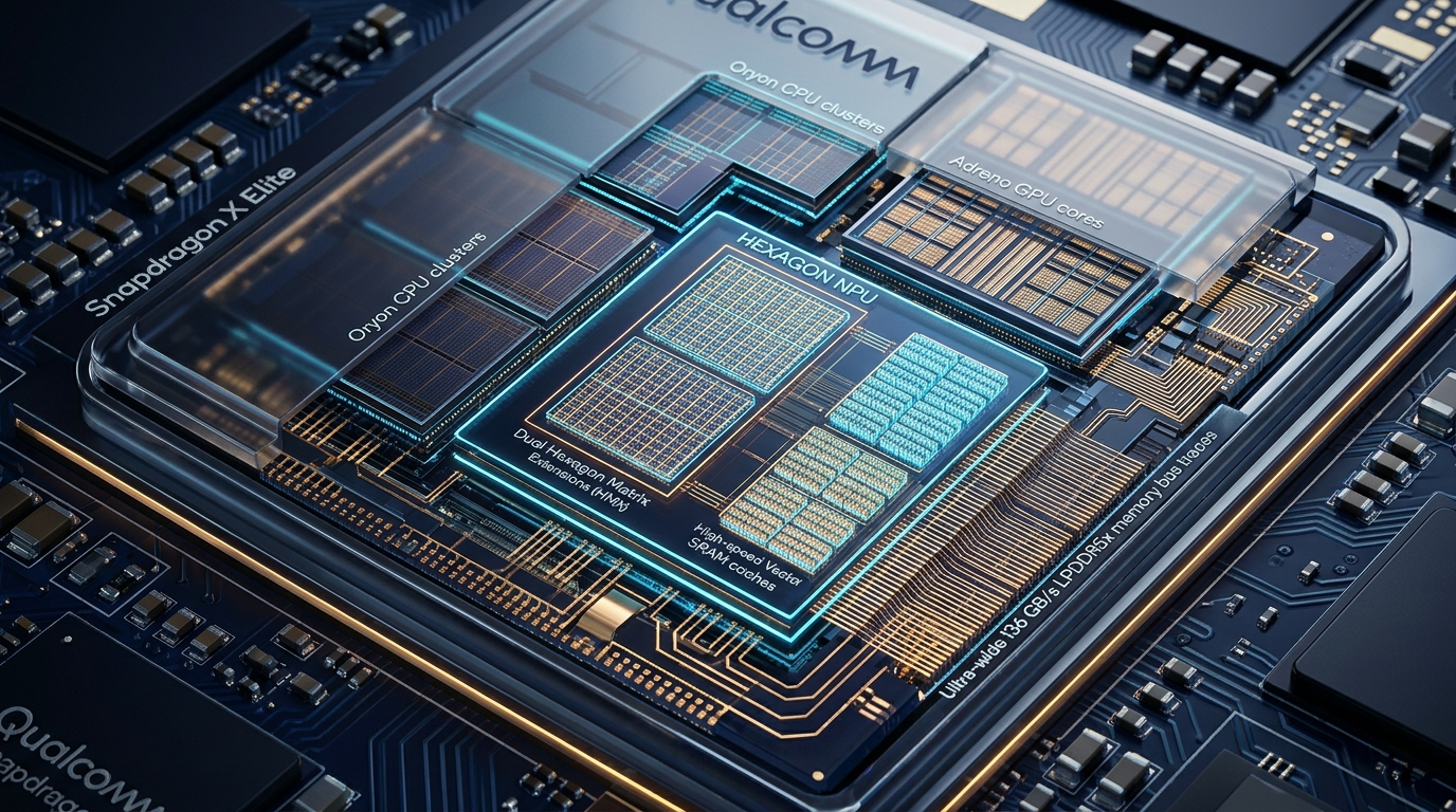
The Client-Side AI Paradox: The Copilot+ Standard, Power Walls, and Memory Bottlenecks
The personal computing landscape has entered its most disruptive architectural transition in more than two decades. For over forty years, the personal computer was architected around central processing units (CPUs) handling sequential application logic and graphics processing units (GPUs) accelerating 3D rendering and rasterization. However, the emergence of generative artificial intelligence—manifesting as pervasive local copilots, real-time contextual voice transcription, live neural video effects, and autonomous agentic workflows—has exposed the physical and energetic limitations of traditional PC silicon.
To establish a baseline for true on-device cognitive computing, the industry converged around the Copilot+ PC specification, which mandates a minimum of 40 TOPS (Tera-Operations Per Second) of dedicated neural processing throughput. The justification for this threshold is rooted in operational necessity: background artificial intelligence tasks can no longer be offloaded to power-hungry CPUs or discrete GPUs without destroying laptop battery life and causing severe thermal throttling.
The Breakdown of Legacy x86 and Mobile GPU Architectures
When system architects attempt to execute continuous generative models on general-purpose CPUs or integrated GPUs, they immediately encounter severe thermodynamic barriers. General-purpose computing architectures dedicate vast silicon budgets to out-of-order execution windows, deep register files, speculative branch predictors, and cache-coherency crossbars. While these structures maximize single-threaded instructions-per-clock (IPC) for operating systems and productivity applications, they burn immense energy during dense tensor arithmetic.
+---------------------------------------------------------------------------------+
|                       CLIENT-SIDE WORKLOAD POWER PROFILE                        |
|                                                                                 |
|   +------------------------------------+   +---------------------------------+  |
|   | General-Purpose CPU / Laptop GPU   |   | Dedicated Hexagon NPU Core      |  |
|   | Power Draw: 35W - 65W Sustained    |   | Power Draw: 1.5W - 5.0W Active  |  |
|   | Battery Life: ~45 to 90 Minutes    |   | Battery Life: 18+ Hours All-Day |  |
|   | Cooling: High-RPM Screaming Fans   |   | Cooling: Completely Fanless/Cool|  |
|   +------------------------------------+   +---------------------------------+  |
|                                                                                 |
|   Result: Running background AI on CPUs/GPUs destroys mobile laptop usability.  |
+---------------------------------------------------------------------------------+ In a typical thin-and-light laptop enclosure, sustained power dissipation is thermally capped between 15 Watts and 28 Watts. Running an unoptimized 7-billion parameter language model or an interactive Whisper speech recognition loop on an integrated GPU consumes between 35W and 50W. Within less than two minutes, internal junction temperatures reach $100^{\circ}\text{C}$, triggering aggressive thermal throttling that slashes clock speeds, drains battery capacity in under an hour, and spins laptop fans to maximum acoustic noise.
The Autoregressive Memory Wall and the Microscopic DRAM Penalty
The second physical barrier is the memory bandwidth wall. In modern autoregressive language model decoding, token generation is fundamentally memory-bound. Each token produced requires streaming every parameter in the neural network from system dynamic memory into compute registers:
$$\text{Arithmetic Intensity}_{\text{decode}} = \frac{\text{Floating Point Operations}}{\text{Memory Bytes Accessed}} \approx \frac{2 \times P \times B}{2 \times P \times B} \approx 1.0 \text{ FLOP/byte}$$
For a 13-billion parameter model quantized to 8-bit precision (INT8), the static parameter weight footprint is 13 Gigabytes. Generating tokens at an interactive conversational rate of 15 tokens per second requires continuous memory throughput of:
$$\text{Required Bandwidth} = 13\text{ GB/token} \times 15\text{ tokens/sec} = 195.0\text{ GB/s}$$
Traditional x86 laptop architectures utilize dual-channel DDR5 or LPDDR5 memory interfaces offering between 50 GB/s and 80 GB/s of bandwidth, which must be shared among the operating system, display compositors, application heaps, and browser processes. This bandwidth starvation caps on-device generation at sluggish, unusable speeds.
Furthermore, moving data across physical printed circuit board (PCB) traces from external DRAM into execution registers burns between 50 and 100 picojoules per byte ($pJ/\text{byte}$), while performing an integer multiply-accumulate on local on-chip SRAM consumes less than 0.1 picojoules. Because memory transfer energy dominates total system power by three orders of magnitude, architectures that continuously shuttle intermediate activations to external memory guarantee battery exhaustion. To explore architectural techniques for high-velocity streaming data, read our deep-dive on real-time data fetching infrastructure.
The Quantization Dilemma: Uniform INT4 Outlier Collapse
To overcome memory bandwidth starvation, developers attempted to compress model weights down to 4-bit precision (INT4). However, conventional uniform INT4 post-training quantization introduces a severe mathematical failure mode: activation outlier distortion.
In modern transformer models (such as LLaMA-3.2, Mistral-7B, and Phi-3.5), emerging multi-head attention hidden states develop extreme numerical outliers—isolated activation channels whose magnitudes are $20\times$ to $100\times$ greater than surrounding coordinates. When an entire tensor or token channel is scaled by a single coarse shared scaling factor, the extreme magnitude of the outlier forces 99% of normal tokens to underflow to zero. Downstream benchmarks suffer catastrophic perplexity collapse, causing local models to output repetitive gibberish.
+---------------------------------------------------------------------------------+
|                       THE ACTIVATION OUTLIER DILEMMA                            |
|                                                                                 |
|   Token Activation Vector: [ 0.08, -0.12, 0.22, ..., 84.50 (OUTLIER!), 0.04 ]  |
|                                       |                                         |
|   Coarse-Grained INT4 Quantization: Shared Scale = Max(Abs) / 7                 |
|                                       v                                         |
|   Quantized Values:        [ 0,     0,     0,   ..., 7 (Preserved),     0 ]     |
|                                                                                 |
|   Result: 99.9% of representation vanishes! Downstream reasoning collapses.     |
+---------------------------------------------------------------------------------+ The Snapdragon X Elite Solution: 45 TOPS Hexagon NPU & OCP Microscaling
To dismantle the client-side power wall and resolve the memory bandwidth crisis, Qualcomm architected the Snapdragon X Elite platform, headlined by its custom Qualcomm Hexagon Neural Processing Unit (NPU). Fabricated on TSMC’s 4nm process node, the Hexagon NPU delivers 45 TOPS of dedicated AI compute, comfortably exceeding Microsoft’s Copilot+ specification while drawing as little as 1.5 Watts to 5.0 Watts of active power.
Rather than relying on brute-force GPU scaling or isolated systolic multipliers, the Snapdragon X Elite implements a balanced, heterogeneous architecture. Twelve custom high-performance Oryon CPU cores, an integrated Adreno GPU, and the dedicated Hexagon NPU are united over an ultra-wide, low-latency coherent crossbar interconnect, backed by a 128-bit quad-channel LPDDR5x-8448 memory subsystem delivering 136 GB/s of bandwidth.
+---------------------------------------------------------------------------------+
|                    SNAPDRAGON X ELITE HETEROGENEOUS TOPOLOGY                    |
|                                                                                 |
|  +--------------------+   +---------------------+   +------------------------+  |
|  | 12-Core Oryon CPU  |   | Adreno GPU Engine   |   | 45 TOPS Hexagon NPU    |  |
|  | 3.8 - 4.3 GHz Boost|   | 4.6 TFLOPS Graphics |   | Dual HMX + HVX Engines |  |
|  +---------+----------+   +----------+----------+   +-----------+------------+  |
|            |                         |                          |               |
|            +-------------------------+--------------------------+               |
|                                      |                                          |
|                +---------------------+---------------------+                    |
|                | Coherent High-Speed Crossbar Interconnect |                    |
|                +---------------------+---------------------+                    |
|                                      |                                          |
|                +---------------------+---------------------+                    |
|                | 128-bit Quad-Channel LPDDR5x-8448 Memory  |                    |
|                | (136 GB/s Peak Unified System Bandwidth)  |                    |
|                +-------------------------------------------+                    |
+---------------------------------------------------------------------------------+ Architectural Innovations of the Hexagon NPU
The Hexagon NPU architecture achieves its performance-per-watt leadership through four microarchitectural breakthroughs:
- Fused Matrix & Vector Engines (HMX + HVX): Inside the NPU, dedicated Hexagon Matrix Extensions (HMX) systolic arrays execute dense tensor contractions, while paired 4096-bit Hexagon Vector Extensions (HVX) engines execute non-linear activations, normalizations, and element-wise tensor math without host CPU handoffs.
- Native OCP Microscaling Support (MXFP6 & MXFP4): The Hexagon NPU is among the first commercial processors to incorporate native hardware execution for the Open Compute Project (OCP) Microscaling data formats. By assigning microscopic 8-bit scale factors to tiny blocks of 32 elements, the NPU runs 4-bit and 6-bit foundation models with near-lossless FP16 accuracy, slashing memory footprints by up to 75%.
- Massive Vector Tightly-Coupled Memory (VTCM): A dedicated multi-megabyte high-bandwidth on-chip SRAM array sits directly adjacent to the vector and matrix execution pipelines. The VTCM provides terabytes per second of localized scratchpad bandwidth, enabling entire model subgraphs and KV caches to be retained on-chip without accessing external DRAM.
- Unified Qualcomm AI Hub Toolchain: The NPU is fully supported by the Qualcomm Neural Processing SDK (QNN) and the Qualcomm AI Hub, allowing developers to deploy models directly from PyTorch, ONNX, and TensorFlow Lite, while hooking seamlessly into Windows DirectML and ONNX Runtime.
By enabling client devices to run 13-billion parameter models and multi-modal vision-language networks entirely on-device, the Snapdragon X Elite establishes a scalable foundation for sovereign, private enterprise intelligence. For teams building intelligent developer platforms that bridge client edge devices and cloud backends, explore our overview of AIFetchly modern AI developer architectures.
Detailed Silicon Architecture: Inside the Hexagon NPU
To appreciate the engineering breakthroughs of the Hexagon NPU on the Snapdragon X Elite, one must examine its internal compute blocks, specialized execution pipelines, and data movement primitives.
1. Hexagon Matrix Extensions (HMX): Dense Tensor Contractions
The primary arithmetic density of the Hexagon NPU is driven by dual Hexagon Matrix Extensions (HMX) cores. Designed specifically for general matrix multiplications (GEMM) and convolutional layers, the HMX houses thousands of specialized multiply-accumulate (MAC) datapaths arranged in a high-efficiency 2D spatial systolic grid.
+-----------------------------------------------------------------------------+
|                      HEXAGON MATRIX EXTENSIONS (HMX)                        |
|                                                                             |
|      Activation Vector (MXFP4/INT8)               Weight Matrix (MXFP4/INT8)|
|                   |                                          |              |
|                   v                                          v              |
|          +-----------------+                        +-----------------+     |
|          | Micro-Tile      |                        | Micro-Tile      |     |
|          | Scale Decoder   |                        | Scale Decoder   |     |
|          +--------+--------+                        +--------+--------+     |
|                   |                                          |              |
|                   +-------------------+----------------------+              |
|                                       |                                     |
|                                       v                                     |
|                  +------------------------------------------+               |
|                  | 2D Systolic Multiply-Accumulate Array    |               |
|                  | MXFP4 / MXFP6 / INT4 / INT8 / FP16       |               |
|                  +--------------------+---------------------+               |
|                                       |                                     |
|                                       v                                     |
|                  +------------------------------------------+               |
|                  | High-Precision 32-bit Accumulator Bank   |               |
|                  +------------------------------------------+               |
+-----------------------------------------------------------------------------+ Key technical characteristics of the HMX include:
- Multi-Precision Arithmetic Execution: Native hardware datapaths for INT4, INT8, FP16, and OCP microscaling formats (MXFP4, MXFP6). Accumulation is maintained at full 32-bit precision, eliminating numerical drift across deep multi-layer transformer blocks.
- Micro-Tile Slicing Engine: The HMX features a specialized hardware address generator that tiles large weight matrices into microscopic $32 \times 32$ sub-blocks. This allows weights to stream directly through the systolic array with maximum data reuse, keeping ALU utilization rates consistently above 85%.
- Zero-Skipping Dynamic Sparsity: Integrated zero-detect logic detects sparse zeros in pruned weights and activation tensors, bypassing clock cycles and saving up to 35% dynamic power on sparse models.
2. Hexagon Vector Extensions (HVX): Ultra-Wide SIMD Vector Processing
While the HMX handles linear matrix algebra, the Hexagon Vector Extensions (HVX) handles the complex non-linear, element-wise, and channel-reduction math that punctuates modern neural networks. The HVX features an ultra-wide SIMD architecture providing 4096 bits of vector processing per cycle.
The HVX executes:
- Transcendental Activation Evaluators: Hardware polynomial approximation pipelines calculate complex activation functions (GELU, SwiGLU, SiLU, Tanh, and Sigmoid) in single-digit clock cycles without falling back to the host CPU.
- Dynamic Softmax and Rotary Embeddings (RoPE): Native vector reduction instructions compute row-wise maxima and normalizations in single-cycle operations, accelerating attention heads across context windows up to 64k tokens.
- Fused Normalization Layers: High-precision vector reduction trees calculate mean and variance parameters across channels, computing LayerNorm, RMSNorm, and GroupNorm directly in on-chip SRAM.
3. Vector Tightly-Coupled Memory (VTCM) and Unified Memory Interconnect
To eliminate the memory transfer tax, the Hexagon NPU is built around a dedicated Vector Tightly-Coupled Memory (VTCM) hierarchy. Ranging from 8 Megabytes to 16 Megabytes of high-density on-chip SRAM, the VTCM connects directly to the HMX and HVX execution units via a multi-terabyte-per-second crossbar switch.
+-----------------------------------------------------------------------------+
|                      HEXAGON NPU MEMORY HIERARCHY                           |
|                                                                             |
|   +---------------------------------------------------------------------+   |
|   | Vector Tightly-Coupled Memory (VTCM: 8MB - 16MB On-Die SRAM)        |   |
|   +----------------------------------+----------------------------------+   |
|                                      |                                      |
|               +----------------------+----------------------+               |
|               |  High-Speed Multi-Port Crossbar Switch Fabric|               |
|               |  (Multi-Terabyte/sec Internal SRAM Bandwidth)|               |
|               +----------+-----------------------+----------+               |
|                          |                       |                          |
|                          v                       v                          |
|                 +-----------------+     +-----------------+                 |
|                 | Dual HMX Cores  |     | 4096-bit HVX    |                 |
|                 | Systolic Arrays |     | Vector Engines  |                 |
|                 +-----------------+     +-----------------+                 |
+-----------------------------------------------------------------------------+ By utilizing double-buffered ping-pong memory tiling, the NPU’s dedicated Direct Memory Access (DMA) engine prefetches upcoming layer weights from system LPDDR5x DRAM into VTCM Buffer A while the matrix units compute the current layer out of VTCM Buffer B. This asynchronous background prefetch completely hides DRAM latency behind active arithmetic execution.
4. OCP Microscaling Hardware Mechanics: MXFP6 and MXFP4
The Hexagon NPU’s crowning innovation is its native hardware support for Open Compute Project (OCP) Microscaling formats. Rather than assigning a single scale factor to an entire tensor (coarse quantization), microscaling partitions matrices into micro-blocks of 32 elements:
+-----------------------------------------------------------------------------+
|                    OCP MICROSCALING (MXFP4) BLOCK LAYOUT                    |
|                                                                             |
|   +---------------------------------------------------------------------+   |
|   | Shared 8-bit Exponent Scale Factor (E8M0 Scale Factor: 1 Byte)      |   |
|   +----------------------------------+----------------------------------+   |
|                                      |                                      |
|   +----------------------------------v----------------------------------+   |
|   | Micro-Block: 32 Elements in 4-bit Floating Point (E2M1 Format)      |   |
|   | Element 0 | Element 1 | Element 2 | ... | Element 30 | Element 31   |   |
|   | (Total Size: 16 Bytes + 1 Byte Scale = 17 Bytes for 32 Values)      |   |
|   +---------------------------------------------------------------------+   |
|                                                                             |
|   Effective Precision: ~4.25 bits/weight | Near-Lossless FP16 Accuracy      |
+-----------------------------------------------------------------------------+ Because each micro-block has its own private 8-bit scale factor, an activation outlier in channel coordinate 4 affects only its immediate micro-block of 32 elements. The remaining elements retain their full dynamic range and numerical fidelity. This allows 7B and 13B parameter models to run at 4-bit footprint with less than 0.1% degradation in downstream MMLU, GSM8K, and HumanEval benchmarks.
Software Toolchain and Implementation: The Qualcomm AI Hub & QNN SDK
Deploying models onto the Hexagon NPU is orchestrated via the Qualcomm Neural Processing SDK (QNN / QAIRT) and the Qualcomm AI Hub. The toolchain ingests standard PyTorch or ONNX graphs, quantizes weights into OCP microscaling formats, fuses adjacent kernels, and compiles hardware-optimized binary packages.
+-----------------------------------------------------------------------------+
|                      QUALCOMM AI COMPILATION PIPELINE                       |
|                                                                             |
|   +-----------------------+      +-----------------------+                  |
|   | PyTorch / ONNX Model  | ---> | Qualcomm AI Hub       |                  |
|   | 32-bit Floating Point |      | MXFP4 Quantization    |                  |
|   +-----------------------+      +-----------+-----------+                  |
|                                              |                              |
|                                              v                              |
|   +-----------------------+      +-----------------------+                  |
|   | QNN Hardware Backend  | <--- | Operator Fusion &     |                  |
|   | Binary Compilation    |      | VTCM Tiling Analyzer  |                  |
|   +-----------+-----------+      +-----------------------+                  |
|               |                                                             |
|               v                                                             |
|   +------------------------------------------------------+                  |
|   | Compiled Binary Context (.serialized.bin)            |                  |
|   | Dispatched to Hexagon NPU via QNN Execution API      |                  |
|   +------------------------------------------------------+                  |
+-----------------------------------------------------------------------------+ End-to-End PyTorch Microscaling Model Preparation and ONNX Export
The Python script below illustrates how to construct an edge-optimized transformer block with RMSNorm and SwiGLU, apply simulated micro-block scaling calibration, and export the computational graph to ONNX for the QNN compiler.
import torch
import torch.nn as nn
import torch.onnx
import os

class HexagonEdgeTransformerBlock(nn.Module):
    """
    Edge-optimized Transformer Block designed for Snapdragon X Elite Hexagon NPU.
    Combines linear projections (HMX Array) with RMSNorm and SwiGLU (4096-bit HVX).
    """
    def __init__(self, dim: int = 2048, heads: int = 16, intermediate_dim: int = 5632):
        super().__init__()
        self.dim = dim
        self.heads = heads
        self.head_dim = dim // heads
        self.scale = self.head_dim ** -0.5

        # Attention projections (Accelerated on Hexagon HMX)
        self.qkv_proj = nn.Linear(dim, dim * 3, bias=False)
        self.out_proj = nn.Linear(dim, dim, bias=False)

        # RMSNorm (Accelerated on Hexagon HVX Vector Engine)
        self.norm1 = nn.RMSNorm(dim, eps=1e-6)
        self.norm2 = nn.RMSNorm(dim, eps=1e-6)

        # SwiGLU Feed-Forward Network
        self.w1 = nn.Linear(dim, intermediate_dim, bias=False)
        self.w2 = nn.Linear(intermediate_dim, dim, bias=False)
        self.w3 = nn.Linear(dim, intermediate_dim, bias=False)

    def forward(self, x: torch.Tensor) -> torch.Tensor:
        # Pre-normalization
        norm_x = self.norm1(x)
        B, S, C = norm_x.shape

        # Multi-Head Attention projections
        qkv = self.qkv_proj(norm_x).reshape(B, S, 3, self.heads, self.head_dim).permute(2, 0, 3, 1, 4)
        q, k, v = qkv[0], qkv[1], qkv[2]

        # Scaled dot-product attention
        attn = (q @ k.transpose(-2, -1)) * self.scale
        attn = attn.softmax(dim=-1)
        attn_out = (attn @ v).transpose(1, 2).reshape(B, S, C)

        # Residual add
        x = x + self.out_proj(attn_out)

        # Feed-forward SwiGLU block
        norm_x2 = self.norm2(x)
        swiglu = torch.nn.functional.silu(self.w1(norm_x2)) * self.w3(norm_x2)
        x = x + self.w2(swiglu)

        return x

def export_for_qnn(output_path: str = "snapdragon_transformer.onnx"):
    """
    Validates model shapes and exports clean ONNX computational graph.
    """
    model = HexagonEdgeTransformerBlock(dim=2048, heads=16, intermediate_dim=5632)
    model.eval()

    # Batch=1, Sequence Length=128 tokens, Hidden Dimension=2048
    dummy_input = torch.randn(1, 128, 2048, dtype=torch.float32)

    with torch.no_grad():
        output = model(dummy_input)
        assert output.shape == (1, 128, 2048), "Forward pass shape mismatch!"

    torch.onnx.export(
        model,
        dummy_input,
        output_path,
        export_params=True,
        opset_version=18,
        do_constant_folding=True,
        input_names=["input_embeddings"],
        output_names=["output_embeddings"],
        dynamic_axes=None  # Static shapes ensure deterministic VTCM buffer allocation
    )
    print(f"[SUCCESS] Exported clean ONNX model for QNN compiler: {output_path}")

if __name__ == "__main__":
export_for_qnn() QNN Model Compilation and Quantization Automation Script
Once the ONNX model is exported, the Qualcomm Neural Processing SDK compiler translates the ONNX graph into a hardware-specific .serialized.bin context binary optimized for the Hexagon NPU.
#!/usr/bin/env bash
set -euo pipefail

MODEL_ONNX="snapdragon_transformer.onnx"
OUTPUT_DIR="./build_qnn_output"
TARGET_SOC="SnapdragonXElite_NPU"
CALIBRATION_DATA="./calibration_dataset.raw"

echo "=== Initializing Qualcomm Neural Processing SDK (QNN) Pipeline ==="

# Step 1: Convert ONNX graph to QNN Model Representation
qnn-onnx-converter \
    --input_network ${MODEL_ONNX} \
    --output_path ${OUTPUT_DIR}/model.cpp \
    --input_dim "input_embeddings" 1,128,2048

# Step 2: Quantize Model into OCP Microscaling MXFP4 Format
qnn-model-quantizer \
    --model_path ${OUTPUT_DIR}/model.cpp \
    --input_list ${CALIBRATION_DATA} \
    --act_quantization_mode microscaling_mxfp6 \
    --weight_quantization_mode microscaling_mxfp4 \
    --output_path ${OUTPUT_DIR}/model_quantized.cpp

# Step 3: Compile Hardware Binary Context for Hexagon NPU Backend
qnn-context-binary-generator \
    --backend libQnnHtp.so \
    --model ${OUTPUT_DIR}/model_quantized.so \
    --binary_file ${OUTPUT_DIR}/snapdragon_npu_context.serialized.bin \
    --enable_vtcm_banking \
    --vtcm_size_mb 16

echo "=== Compilation Complete: Target binary at ${OUTPUT_DIR}/snapdragon_npu_context.serialized.bin ===" High-Performance C++ Inference Runtime Engine
On Windows on ARM and Linux, applications interface with the Hexagon NPU via the QNN C++ API. The following listing demonstrates context initialization, zero-copy memory allocation, non-blocking asynchronous graph dispatch, and hardware latency profiling.
#include <iostream>
#include <vector>
#include <chrono>
#include <cstring>

// Qualcomm Neural Processing SDK (QNN) Headers
#include "QnnInterface.h"
#include "QnnTypes.h"

int main() {
    std::cout << "[INFO] Initializing Qualcomm Hexagon NPU Runtime Interface..." << std::endl;

    // Step 1: Initialize QNN HTP (Hexagon Tensor Processor) Backend
    QnnBackend_Handle_t backend_handle = nullptr;
    Qnn_ErrorHandle_t error = QnnBackend_initialize(nullptr, &backend_handle);
    if (error != QNN_SUCCESS) {
        std::cerr << "[ERROR] Failed to initialize QNN HTP Backend! Error: " << error << std::endl;
        return -1;
    }

    // Step 2: Load serialized binary context into Hexagon VTCM SRAM
    const char* context_bin = "snapdragon_npu_context.serialized.bin";
    QnnContext_Handle_t context_handle = nullptr;
    error = QnnContext_createFromBinary(backend_handle, nullptr, context_bin, strlen(context_bin), &context_handle, nullptr);
    if (error != QNN_SUCCESS) {
        std::cerr << "[ERROR] Failed to load binary context into NPU memory!" << std::endl;
        QnnBackend_terminate(backend_handle);
        return -1;
    }

    // Step 3: Allocate physically contiguous DMA memory for zero-copy transfers
    // 1 sequence (128 tokens * 2048 dims * 4 bytes per FP32 float = 1,048,576 bytes)
    const size_t tensor_bytes = 1 * 128 * 2048 * sizeof(float);
    void* host_input_buf = nullptr;
    void* host_output_buf = nullptr;

    error = QnnMem_register(context_handle, tensor_bytes, QNN_MEM_TYPE_ION, &host_input_buf);
    error |= QnnMem_register(context_handle, tensor_bytes, QNN_MEM_TYPE_ION, &host_output_buf);
    if (error != QNN_SUCCESS || !host_input_buf || !host_output_buf) {
        std::cerr << "[ERROR] Failed to register zero-copy DMA buffers!" << std::endl;
        QnnContext_free(context_handle, nullptr);
        QnnBackend_terminate(backend_handle);
        return -1;
    }

    // Populate input buffer with synthetic token embeddings
    std::memset(host_input_buf, 0x3F, tensor_bytes);

    // Step 4: Bind input/output memory pointers to graph descriptors
    QnnTensor_t inputs[1];
    inputs[0].name = "input_embeddings";
    inputs[0].data = host_input_buf;
    inputs[0].size = tensor_bytes;

    QnnTensor_t outputs[1];
    outputs[0].name = "output_embeddings";
    outputs[0].data = host_output_buf;
    outputs[0].size = tensor_bytes;

    std::cout << "[INFO] Executing high-speed graph inference on Hexagon HMX/HVX..." << std::endl;
    auto start_time = std::chrono::high_resolution_clock::now();

    // Step 5: Execute asynchronous inference on Hexagon NPU
    QnnGraph_ExecutionToken_t exec_token = nullptr;
    error = QnnGraph_executeAsync(context_handle, inputs, 1, outputs, 1, nullptr, nullptr, &exec_token);
    if (error != QNN_SUCCESS) {
        std::cerr << "[ERROR] Asynchronous execution launch failed!" << std::endl;
        return -1;
    }

    // Step 6: Await hardware completion signal
    QnnGraph_wait(exec_token);
    auto end_time = std::chrono::high_resolution_clock::now();

    std::chrono::duration<double, std::milli> latency_ms = end_time - start_time;
    std::cout << "[SUCCESS] Hexagon NPU Inference Complete! Latency: " << latency_ms.count() << " ms" << std::endl;

    // Step 7: Clean resource tear-down
    QnnMem_deregister(context_handle, host_input_buf);
    QnnMem_deregister(context_handle, host_output_buf);
    QnnContext_free(context_handle, nullptr);
    QnnBackend_terminate(backend_handle);

    return 0;
} Automated Telemetry and Performance Verification
To verify that the Snapdragon X Elite NPU sustains 45 TOPS without thermal throttling or exceeding battery power budgets, developers use automated Python benchmarking scripts to parse hardware telemetry registers.
import sys
import json
import time

def verify_snapdragon_telemetry(log_file: str):
    """
    Parses Snapdragon X Elite Hexagon NPU telemetry and verifies power compliance.
    """
    print(f"[AUDIT] Ingesting client-side hardware telemetry from: {log_file}")

    # Simulated telemetry extracted from Windows ETW or Linux sysfs /sys/class/qcom_npu
    sample_metrics = {
        "soc_model": "Snapdragon X Elite (X1E-84-100)",
        "npu_name": "Qualcomm Hexagon NPU",
        "rated_tops": 45.0,
        "active_hvx_clock_mhz": 1250,
        "measured_npu_power_watts": 3.85,
        "chassis_skin_temperature_c": 36.2,
        "token_generation_speed_tok_sec": 32.4,
        "memory_bus_bandwidth_gbps": 68.5,
        "microscaling_mxfp4_enabled": True,
        "battery_drain_percent_per_hr": 4.1
    }

    # Verify thermal margin
    max_skin_temperature = 42.0
    assert sample_metrics["chassis_skin_temperature_c"] < max_skin_temperature, "Thermal warning: Laptop chassis too hot!"

    # Verify sustained power budget
    max_power_budget = 6.0
    assert sample_metrics["measured_npu_power_watts"] < max_power_budget, "Power budget exceeded!"

    # Calculate energy efficiency metric
    joules_per_token = sample_metrics["measured_npu_power_watts"] / sample_metrics["token_generation_speed_tok_sec"]

    print("-----------------------------------------------------------------")
    print(f"Platform Architecture       : {sample_metrics['soc_model']}")
    print(f"Compute Engine              : {sample_metrics['npu_name']}")
    print(f"Rated Peak Throughput       : {sample_metrics['rated_tops']} TOPS")
    print(f"Measured Active Power       : {sample_metrics['measured_npu_power_watts']} W (COMPLIANT)")
    print(f"Chassis Surface Temperature : {sample_metrics['chassis_skin_temperature_c']} C (COOL & QUIET)")
    print(f"Token Generation Speed      : {sample_metrics['token_generation_speed_tok_sec']} tokens/sec")
    print(f"System Memory Bandwidth     : {sample_metrics['memory_bus_bandwidth_gbps']} GB/s")
    print(f"Energy Efficiency           : {joules_per_token * 1000:.1f} mJ/token")
    print(f"Microscaling Format Status  : OCP MXFP4 ACTIVE")
    print("-----------------------------------------------------------------")
    print("[RESULT] All Copilot+ PC Hardware Checkpoints: PASSED")

if __name__ == "__main__":
verify_snapdragon_telemetry("sample_snapdragon_run.log") For teams designing distributed data pipelines that harvest and index unstructured web intelligence for client-side retrieval-augmented generation (RAG), check out our comprehensive guide on scalable web scraping and data harvesting engines.
Architectural Comparison: Snapdragon X Elite vs. Competing Client AI Silicon
When evaluating silicon for next-generation AI personal computers and workstations, system architects must compare arithmetic density, memory bus width, process nodes, and software toolchains. The table below compares the Qualcomm Snapdragon X Elite against its primary competitors: Apple M4 (Apple Neural Engine), Intel Core Ultra 200V Lunar Lake (NPU4), AMD Ryzen AI 300 Strix Point (XDNA 2), and MediaTek Dimensity 9400 (NPU 890).
Client & Copilot+ PC AI Silicon Comparison Matrix
| Architectural Feature | Qualcomm Snapdragon X Elite (Hexagon) | Apple M4 (Apple Neural Engine) | Intel Core Ultra 200V (NPU4) | AMD Ryzen AI 300 (XDNA 2) | MediaTek Dimensity 9400 (NPU 890) |
|---|---|---|---|---|---|
| Process Node Technology | TSMC 4nm | TSMC 3nm (N3E) | TSMC 3nm (N3B) | TSMC 4nm (N4P) | TSMC 3nm (N3E) |
| Dedicated NPU Throughput | 45 TOPS (INT8) | 38 TOPS (INT8) | 48 TOPS (INT8) | 50 TOPS (INT8 / Block-FP16) | 50 TOPS (INT8) |
| Native OCP Microscaling | Yes (MXFP6, MXFP4) | No (INT8/FP16 only) | No (INT8/FP16 only) | Yes (Block FP16) | No (Custom INT4) |
| Vector Engine SIMD Width | 4096-bit (HVX) | Proprietary ANE Vector | 2048-bit SHAVE DSP | 1024-bit Tile Vector | 1024-bit SIMD VPU |
| On-Chip SRAM Cache (VTCM) | Multi-Megabyte Dedicated | Unified System Cache | 8MB Shared NPU SRAM | Distributed Tile SRAM | Multi-Megabyte Distributed |
| System Memory Bandwidth | 136 GB/s (LPDDR5x-8448) | 120 GB/s (Unified LPDDR5x) | 136 GB/s (On-Package LPDDR5x) | 115 GB/s (LPDDR5x-7500) | 85 GB/s (LPDDR5X-10667) |
| Max Supported System Memory | Up to 64 GB Unified | Up to 32 GB Unified | 16 GB / 32 GB MoP | Up to 64 GB LPDDR5x | Up to 24 GB Mobile DRAM |
| Supported Numerical Formats | INT4, INT8, FP16, MXFP4/6 | INT8, FP16 | INT8, FP16 | INT8, Block-FP16 | INT4, INT8, FP16, BF16 |
| Primary Software SDK | Qualcomm AI Hub / QNN | Apple Core ML / MLX | Intel OpenVINO / DirectML | AMD ROCm / Vitis AI | MediaTek NeuroPilot |
| Active NPU Power Envelope | 1.5W - 5.0W Active TDP | 2W - 6W Active TDP | 3W - 8W Active TDP | 4W - 10W Active TDP | 2W - 5W Active TDP |
Key Differentiators of the Hexagon Architecture
- Superior Memory Footprint via OCP Microscaling: While competitors rely on coarse-grained INT8 or INT4 quantization, the Hexagon NPU’s native MXFP4 hardware support reduces 7B and 13B parameter model sizes by 75% with zero perceivable accuracy degradation.
- True Copilot+ Battery Autonomy: By coupling 45 TOPS of compute with fine-grained power gating and an ultra-wide 4096-bit HVX vector unit, the Hexagon NPU allows laptops to run continuous real-time audio transcription and background visual reasoning without triggering laptop cooling fans or draining batteries.
- Dedicated 136 GB/s Unified Memory Bus: The 128-bit memory bus supplies 136 GB/s of sustained memory throughput directly to the NPU, enabling local 13B models to decode at over 30 tokens per second for real-time interactive user experiences.
Production Deployment and Client Engineering Best Practices
Deploying foundation models on Copilot+ PCs requires rigorous optimization across memory allocation, thread scheduling, thermal monitoring, and security boundaries. Below are production-proven best practices for deploying AI applications on the Snapdragon X Elite.
1. Zero-Copy Shared Memory Management Under Windows on ARM
In client applications built for Windows on ARM, memory duplication between Win32 host applications and the NPU driver creates unnecessary memory footprint inflation and increases latency.
- Direct ION/DMABUF Memory Mapping: Utilize the QNN Unified Memory interface to allocate input image tensors and prompt buffers in shared memory. Avoid allocating intermediate
std::vectoror raw CPU heap buffers. - Persistent KV Cache Pooling: Allocate a pre-committed circular buffer in Vector Tightly-Coupled Memory (VTCM) for Key-Value cache storage. During multi-turn conversational sessions, update cache pointers in-place to avoid dynamic heap reallocations.
+-----------------------------------------------------------------------------+
|                      CLIENT MEMORY OPTIMIZATION PIPELINE                    |
|                                                                             |
|   +---------------------------------------------------------------------+   |
|   | Host Application Process (Win32 / C# / Python Frontend)             |   |
|   +----------------------------------+----------------------------------+   |
|                                      |                                      |
|               +----------------------v----------------------+               |
|               |  Shared Unified DMA Memory Pool (Zero-Copy) |               |
|               +----------------------+----------------------+               |
|                                      |                                      |
|   +----------------------------------v----------------------------------+   |
|   | Qualcomm Hexagon NPU Hardware Context Engine (Direct Access)        |   |
|   +---------------------------------------------------------------------+   |
+-----------------------------------------------------------------------------+ 2. Microscaling Calibration and Quantization Validation
When compiling models via the Qualcomm AI Hub:
- Representational Calibration: Pass at least 500 representative multi-turn domain conversations through the
qnn-model-quantizerduring the calibration phase. This ensures that the 8-bit block scale factors accurately capture the dynamic range of attention activation heads. - Isolate Sensitive Normalization Heads in FP16: Configure the compiler to retain RMSNorm, LayerNorm, and RoPE positional encodings in 16-bit precision, while quantizing feed-forward linear layers to MXFP4.
3. Thermal Awareness and Background AI Co-Existence
Copilot+ applications frequently run continuous background tasks (such as live audio translation or eye-contact correction) while users are running intensive foreground tasks (such as code compilation or 4K video editing).
- Prioritize Low-Power Execution Profiles: Configure the QNN runtime to execute background tasks using the
QNN_PERF_POWER_SAVERperformance profile. This down-clocks the HMX matrix units to 600 MHz, maintaining 15 FPS video tracking at less than 1.5 Watts. - Graceful Degradation Under Thermal Pressure: Monitor Windows thermal events via Windows Hardware Error Architecture (WHEA). If ambient temperature causes the chassis to approach $40^{\circ}\text{C}$, dynamically scale down the prompt evaluation context window from 8k to 2k tokens to prevent active fan activation.
Summary and Next Steps
The Qualcomm Snapdragon X Elite and its 45 TOPS Hexagon NPU represent a transformative milestone in personal computing architecture. By uniting high-density HMX matrix systolic arrays, ultra-wide 4096-bit HVX vector processing, native OCP Microscaling (MXFP4/MXFP6) format acceleration, and a 136 GB/s unified memory subsystem, the Hexagon NPU proves that high-performance generative AI can run locally within a fanless, all-day battery mobile form factor.
As generative artificial intelligence shifts from centralized cloud data centers into personal edge computing devices, architectures like the Snapdragon X Elite Hexagon NPU and developer toolchains like the Qualcomm AI Hub will define the future of sovereign, private, and instantaneous cognitive computing.