Rebellions REBEL Guide: 4nm 144GB HBM3e AI Chiplet Silicon
The Monolithic Reticle Barrier and the LLM Memory Wall Crisis
In modern enterprise artificial intelligence platforms, autonomous multi-agent systems, and high-velocity web harvesting infrastructures powered by AI Fetchly, large language models and multimodal foundation networks represent the core computational engine. Whether extracting structured corporate filings through automated data harvesting, orchestrating streaming multi-modal conversational feeds with real-time content ingestion, or executing trillion-parameter Mixture-of-Experts inference pipelines, datacenter infrastructure is undergoing an unprecedented scaling transformation.
However, attempting to serve frontier generative models—such as Llama-3.1 70B, Llama 405B, and complex multi-modal vision-language networks—on traditional monolithic accelerator silicon exposes two catastrophic industry bottlenecks:
1. The Monolithic Reticle Limit and the Semiconductor Yield Trap
For decades, semiconductor performance scaled by designing larger and more complex monolithic silicon dies. However, photolithography systems encounter a fundamental physical constraint known as the photolithographic reticle limit:
- Standard deep-ultraviolet and extreme-ultraviolet lithography scanners can expose a maximum physical field size of approximately 858 square millimeters (typically 26 mm by 33 mm).
- When semiconductor architects design monolithic AI processors pushing against this reticle boundary (such as 800 mm² to 850 mm² dies), semiconductor manufacturing yield plummets exponentially. According to Murphy’s yield model, defect probability increases drastically with die area. A single microscopic dust particle or crystal dislocation anywhere on an 800 mm² wafer surface ruins the entire multi-thousand-dollar die.
- Wafers processed on cutting-edge 4nm and 3nm foundry nodes suffer low mature yields on reticle-limit dies, forcing merchant silicon vendors to charge exorbitant gross-margin premiums to recoup manufacturing scrap costs.
- For enterprise datacenters and national sovereign AI initiatives, paying massive premiums for low-yield monolithic chips creates severe capital expenditure drag, restricting cluster expansion.
2. The Autoregressive Generation Memory Wall
While model pre-training is fundamentally compute-bound (governed by dense matrix multiplications), production inference serving is bound almost entirely by memory capacity and memory bandwidth:
- In autoregressive token generation, language models must load their entire parameter weight matrix from memory into arithmetic execution registers for every single generated token.
- A 70-billion-parameter foundation model running in 16-bit floating-point precision requires 140 gigabytes of memory purely to hold its weights, completely excluding the dynamic Key-Value (KV) cache generated by hundreds of concurrent user requests.
- When serving long-context prompts (such as 32k to 128k context windows), KV-cache allocation rapidly consumes tens to hundreds of gigabytes of additional memory.
- If an accelerator possesses insufficient on-board memory capacity, engineering teams are forced to shard models across multiple separate accelerator cards via tensor parallelism. This introduces high-latency inter-card communication overhead, burning expensive network bandwidth simply to pool fragmented memory.
3. Supply Chain Vulnerability and Sovereign Cloud Pressures
Global enterprise organizations and sovereign governments face growing geopolitical and economic imperatives to establish autonomous AI infrastructure:
- Relying on a single dominant merchant silicon vendor creates severe supply-chain allocation bottlenecks, lead times extending beyond six to twelve months, and proprietary software lock-in.
- To achieve true infrastructure resilience, the enterprise AI ecosystem requires an open, high-yield, standards-based accelerator capable of matching premier merchant GPU performance while delivering superior memory density and total cost of ownership.
+----------------------------------------------------------------------------------------------------+
| THE MONOLITHIC RETICLE LIMIT VS. AUTOREGRESSIVE MEMORY BOTTLENECK                                  |
+----------------------------------------------------------------------------------------------------+
| MONOLITHIC SILICON YIELD CRISIS:                                                                    |
| [Single 800mm² Monolithic Die] ===> High defect vulnerability on 4nm/3nm wafers                   |
| - Low manufacturing yields force multi-thousand-dollar margin premiums on datacenter silicon        |
| - Physical reticle boundaries prevent adding more on-chip compute and memory controller logic       |
|                                                                                                    |
| AUTOREGRESSIVE LLM SERVING BOTTLENECK:                                                             |
| - 70B FP16 Model = 140 GB parameter weights + tens of GBs for dynamic KV-Cache                    |
| - Memory-constrained accelerators (<80GB) force aggressive tensor sharding across multiple cards  |
| - Inter-card communication latency chokes token generation throughput                              |
+----------------------------------------------------------------------------------------------------+ 4. Thermal Throttling and Datacenter Power Distribution Ceilings
Beyond silicon manufacturing defects, commercial hyperscale facilities face rigid infrastructure power boundaries:
- Operating 700-watt to 1,000-watt GPU server trays requires massive facility retrofits, including multi-million-dollar direct-to-chip liquid cooling loops and specialized medium-voltage electrical substations.
- In standard enterprise datacenters limited to 10 to 15 kilowatts per rack, installing high-wattage GPUs results in half-empty server racks, because the electrical circuit breaker capacity is exhausted long before physical rack space is filled.
- High thermal dissipation also induces severe thermal throttling: when junction temperatures approach 80°C under continuous batching inference loads, clock frequencies drop dynamically, introducing unpredictable latency spikes into user-facing production APIs.
- To achieve sustainable inference economics, enterprise datacenters demand high-density AI accelerators that operate within standard 350-watt power envelopes, allowing complete rack saturation on conventional forced-air cooling infrastructure.
Enter Rebellions REBEL: Modular Multi-Chiplet Architecture with Samsung SF4X
To eliminate the monolithic reticle trap and solve the large language model memory wall, South Korean AI semiconductor pioneer Rebellions developed REBEL (RBLN-CR13). Unveiled to the global semiconductor community at Hot Chips 2025, REBEL represents a watershed engineering breakthrough: a high-grade datacenter AI accelerator co-developed in close technological partnership with Samsung Foundry and Samsung Memory.
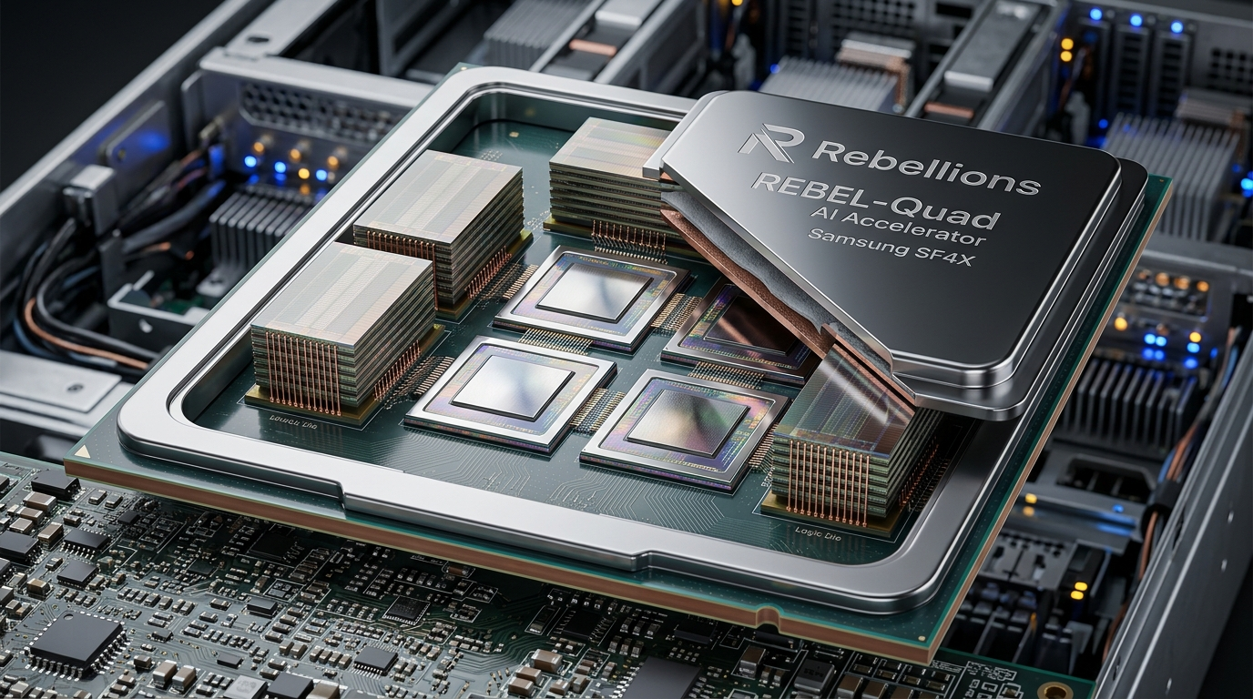
Rather than betting on a single massive, low-yield monolithic die, Rebellions architected REBEL around an advanced modular chiplet paradigm. Fabricated on Samsung Foundry’s advanced 4nm SF4X high-performance computing process, the flagship REBEL-Quad accelerator packages four proven, high-yield NPU compute chiplets (each approximately 320 mm²) onto an advanced 2.5D silicon interposer using Samsung I-Cube (CoWoS-S equivalent) packaging.
Interconnected via standard Universal Chiplet Interconnect Express (UCIe-Advanced) interfaces, the four chiplets function logically as a single unified super-accelerator, delivering 1 PFLOPS of FP16 and 2,048 TFLOPS (2 PFLOPS) of FP8 compute within an air-cooled 350-watt power envelope.
+----------------------------------------------------------------------------------------------------+
| REBELLIONS REBEL-QUAD: 4nm CHIPLET PACKAGING ON 2.5D SILICON INTERPOSER                            |
+----------------------------------------------------------------------------------------------------+
|                                                                                                    |
|    +-------------------------+                     +-------------------------+                     |
|    | HBM3e Memory Stack 0    |                     | HBM3e Memory Stack 1    |                     |
|    | 36 GB (1.2 TB/s BW)     |                     | 36 GB (1.2 TB/s BW)     |                     |
|    +-------------------------+                     +-------------------------+                     |
|                 |                                               |                          |
|                 +-----------------------+-----------------------+                          |
|                                         |                                                  |
|    +----------------------------------------------------------------------------------+    |
|    | FOUR MODULAR NPU CHIPLETS (Samsung 4nm SF4X Node / ~320mm² each)                 |    |
|    |                                                                                  |    |
|    |  +-------------------------+  (11ns UCIe)   +-------------------------+          |    |
|    |  | Compute Chiplet 0       |<=============>| Compute Chiplet 1       |          |    |
|    |  | - Neural Engine Core    |  (16 Gbps D2D)| - Neural Engine Core    |          |    |
|    |  | - 128 MB Local SRAM     |               | - 128 MB Local SRAM     |          |    |
|    |  +-------------------------+               +-------------------------+          |    |
|    |               ^                                   ^                              |    |
|    |               | (~4 TB/s UCIe Mesh Fabric)        | (~4 TB/s UCIe Mesh Fabric)   |    |
|    |               v                                   v                              |    |
|    |  +-------------------------+               +-------------------------+          |    |
|    |  | Compute Chiplet 2       |<=============>| Compute Chiplet 3       |          |    |
|    |  | - Neural Engine Core    |  (16 Gbps D2D)| - Neural Engine Core    |          |    |
|    |  | - 128 MB Local SRAM     |               | - 128 MB Local SRAM     |          |    |
|    |  +-------------------------+               +-------------------------+          |    |
|    +----------------------------------------------------------------------------------+    |
|                                         |                                                  |
|                 +-----------------------+-----------------------+                          |
|                 |                                               |                          |
|    +-------------------------+                     +-------------------------+                     |
|    | HBM3e Memory Stack 2    |                     | HBM3e Memory Stack 3    |                     |
|    | 36 GB (1.2 TB/s BW)     |                     | 36 GB (1.2 TB/s BW)     |                     |
|    +-------------------------+                     +-------------------------+                     |
|                                                                                                    |
|  AGGREGATE MEMORY: 144 GB HBM3e (4.8 TB/s Sustained Bandwidth) | TOTAL ON-CHIP SRAM: 512 MB        |
+----------------------------------------------------------------------------------------------------+ 1. The Chiplet Advantage: Dodging Reticle Limits and Maximizing Yield
By disaggregating a massive 1,280 mm² total compute surface into four ~320 mm² dies, Rebellions completely sidesteps photolithographic reticle limitations:
- High Semiconductor Yields: Smaller 320 mm² chiplets achieve substantially higher wafer yields on Samsung’s 4nm SF4X process, dramatically lowering fabrication costs compared to monolithic reticle-limit chips.
- Standardized UCIe-Advanced Die-to-Die Interconnect: The chiplets communicate across ultra-dense micro-bumps using the open UCIe-Advanced standard. Running at 16 Gbps per pin, the inter-chiplet interface delivers approximately 4 terabytes per second of bidirectional die-to-die bandwidth with an ultra-low latency of 11 nanoseconds.
- Coherent Execution Fabric: The latency of UCIe is so low that software runtimes and neural compilers treat the four distinct chiplets as an unpartitioned, homogeneous matrix of execution units.
2. Massive 144 GB HBM3e Memory Capacity at 4.8 TB/s
Memory starvation is eliminated by surrounding the four compute chiplets with four cutting-edge Samsung HBM3e modules:
- Single-Card Parameter Residence: The four stacks provide an aggregate memory capacity of 144 gigabytes of HBM3e, enabling state-of-the-art 70-billion-parameter foundation models (such as Llama-3.1 70B) to reside entirely on a single accelerator card.
- 4.8 Terabytes per Second Throughput: With an aggregate memory throughput of 4.8 TB/s, REBEL delivers the memory bandwidth necessary to keep arithmetic engines fully saturated during autoregressive token decode phases.
- 512 MB On-Chip SRAM Hierarchy: In addition to HBM3e, REBEL integrates a massive 512 megabytes of ultra-low-latency on-chip SRAM distributed across the four chiplets (128 MB per chiplet), caching frequent activation tensors and KV-cache blocks with single-cycle access latencies.
3. Sovereign AI Consolidation: The Rebellions and Sapeon Merger
In late 2024 and 2025, Rebellions completed a historic merger with Sapeon (the AI chip spin-out of SK Telecom). Backed by South Korea’s telecommunications giants (KT and SK Telecom) and financial institutions:
- The combined entity established a dominant sovereign AI semiconductor champion valued at over $1 billion.
- REBEL serves as the flagship silicon foundation for national AI datacenters, enterprise sovereign clouds, and global export markets, providing an open, high-performance alternative to proprietary merchant silicon.
4. Samsung SF4X Transistor Innovation and Advanced Packaging Synergy
The technical foundation of REBEL rests on close co-development with Samsung Foundry’s dedicated high-performance computing node:
- Samsung SF4X Process Optimization: While consumer mobile processes optimize strictly for low leakage current, SF4X is engineered specifically for high-frequency datacenter operation. It features optimized FinFET fin profiles, low-resistance metal interconnect stacks, and reduced parasitic capacitance, enabling REBEL’s Neural Engine Clusters to operate at elevated clock rates while maintaining strict power efficiency.
- Samsung I-Cube 2.5D Packaging: Samsung’s proprietary I-Cube integration places the four SF4X compute dies and four HBM3e memory stacks side-by-side on a high-density silicon interposer. Microscopic Through-Silicon Vias (TSVs) and fine-pitch micro-bumps ensure pristine signal integrity, allowing 4.8 terabytes per second of memory bandwidth to flow into the compute cores with near-zero transmission losses.
Deep Architectural Analysis of the REBEL Silicon Subsystems
To understand how REBEL achieves high hardware utilization across large language models and multi-modal architectures, we examine its Neural Engine Cluster microarchitecture, on-chip 2D mesh, memory controller integration, and host scale-up interfaces.
+----------------------------------------------------------------------------------------------------+
| DETAILED ARCHITECTURAL BLOCK DIAGRAM: SINGLE REBEL COMPUTE CHIPLET MICROARCHITECTURE               |
+----------------------------------------------------------------------------------------------------+
|                                                                                                    |
|  +----------------------------------------------------------------------------------------------+  |
|  | NEURAL ENGINE CLUSTERS (NEC): Massive Parallel Systolic Array Matrix Processing              |  |
|  | - Matrix Arithmetic Units: Native support for FP16, BF16, FP8, and INT8/INT4 math            |  |
|  | - Vector SIMD Engines: High-speed activation processing (GELU, SwiGLU, LayerNorm, Softmax)   |  |
|  | - Dedicated Attention Acceleration Units: Hardware-accelerated FlashAttention-3 pipelines   |  |
|  +----------------------------------------------------------------------------------------------+  |
|                                                ^                                                   |
|                                                | (Zero-Contention 2D Dense Mesh Interconnect)      |
|                                                v                                                   |
|  +----------------------------------------------------------------------------------------------+  |
|  | DISTRIBUTED ON-CHIP SRAM CACHE (128 MB Local SRAM per Chiplet / 512 MB Across Package)       |  |
|  | - Multi-Terabyte/s Non-Blocking Internal Crossbar Bandwidth                                  |  |
|  | - Local Scratchpad & Activation Buffering caching intermediate attention heads               |  |
|  +----------------------------------------------------------------------------------------------+  |
|                                                ^                                                   |
|                                                | (High-Density Silicon Bridge)                     |
|                                                v                                                   |
|  +----------------------------------------------------------------------------------------------+  |
|  | UCIe-ADVANCED DIE-TO-DIE INTERCONNECT (16 Gbps / ~4 TB/s Inter-Chiplet Bandwidth / ~11ns)    |  |
|  | - Seamless Coherent Memory Addressing across all 4 Chiplets in REBEL-Quad package            |  |
|  +----------------------------------------------------------------------------------------------+  |
|                                                ^                                                   |
|                                                | (Embedded Silicon PHYs)                           |
|                                                v                                                   |
|  +----------------------------------------------------------------------------------------------+  |
|  | EMBEDDED HBM3e CONTROLLER & PHYSICAL LAYER (1.2 TB/s per Stack / 4.8 TB/s Total Subsystem)   |  |
|  +----------------------------------------------------------------------------------------------+  |
|                                                                                                    |
+----------------------------------------------------------------------------------------------------+ 1. Neural Engine Clusters (NEC) and Tensor Compute Units
Within each 320 mm² chiplet, arithmetic processing is structured into Neural Engine Clusters (NECs):
- Systolic Tensor Matrix Units: Optimized for dense matrix multiply-accumulate operations, the tensor units feature high silicon packing density, natively executing FP16, BF16, and FP8 arithmetic. In FP8 mode, REBEL delivers 2,048 TFLOPS of peak inference compute.
- Vector SIMD Execution Pipelines: High-performance deep learning models heavily employ complex activation functions, normalization layers, and positional embeddings (such as SwiGLU, RMSNorm, and Rotary Position Embeddings / RoPE). Dedicated vector SIMD pipelines execute these operations directly alongside the matrix units, preventing memory writeback stalls.
- Hardware-Accelerated FlashAttention Pipelines: Recognizing that attention computation dominates Transformer execution time, REBEL integrates dedicated hardware state-tracking logic designed to execute tiling-based FlashAttention kernels natively, maximizing tensor core arithmetic duty cycles.
2. High-Bandwidth UCIe-Advanced Die-to-Die Interconnect
The four compute chiplets in the REBEL-Quad package communicate across an advanced 2.5D packaging substrate:
- Sub-11-Nanosecond Latency: Utilizing the UCIe-Advanced standard, signals travel across microscopic copper micro-bumps and silicon bridge traces, achieving an unprecedented 11-nanosecond die-to-die latency.
- 4 TB/s Inter-Chiplet Bandwidth: Operating at 16 Gbps per pin across thousands of parallel lanes, the aggregate interconnect bandwidth between chiplets reaches 4 terabytes per second, completely eliminating inter-die communication bottlenecks.
- Unified Virtual Address Space: Memory controllers across all four chiplets map HBM3e modules and local SRAM into a single, contiguous address space with full hardware cache coherency.
3. Integrated HBM3e Memory Controller Architecture
Unlike legacy architectures where memory controllers are located far from compute logic on the chip perimeter, REBEL embeds dedicated HBM3e controllers and physical layers (PHYs) directly adjacent to the Neural Engine Clusters:
- Direct Short-Trace Routing: Silicon interposer traces connecting the compute logic to the four Samsung HBM3e stacks are kept under a few millimeters in length, drastically reducing signal attenuation and dynamic capacitive power dissipation.
- Non-Blocking 2D Mesh Network: On-chip traffic flows across a high-frequency 2D dense mesh network, routing data packets between any HBM3e channel, on-chip SRAM bank, and compute cluster with deterministic, guaranteed latency.
4. Enterprise Host Interfacing and Power Delivery
In commercial datacenter installations:
- PCIe Gen 5 x16 Interface: REBEL interfaces with host CPU servers across a high-speed PCIe Gen 5 x16 bus delivering 128 GB/s of bidirectional host-to-device throughput, equipped with CXL memory-expansion protocol support.
- 350-Watt Power Envelope: Despite packing 144 GB of HBM3e and 2 PFLOPS of compute, REBEL operates within a standard 350W TDP, allowing it to be cooled using standard datacenter forced-air heat sinks or direct-to-chip liquid cooling manifolds.
5. Dense 2D Mesh Network-on-Chip (NoC) and Flow Control
To prevent internal data congestion across the four chiplets, REBEL deploys an ultra-wide Dense 2D Mesh Network-on-Chip (NoC):
- Non-Blocking Credit-Based Flow Control: On-chip packets travel across independent row and column routing rings coordinated by credit-based virtual channels. When high-bandwidth KV-cache blocks stream from HBM3e into local SRAM, the NoC dynamically routes packets around busy arithmetic clusters, preventing pipeline stalls.
- Hardware Prefetch Engines: Each Neural Engine Cluster integrates autonomous hardware prefetch engines that predict upcoming Transformer layer memory access patterns. By pre-staging activation weights from HBM3e into local 512 MB SRAM banks cycles ahead of execution, the arithmetic matrix units maintain continuous execution duty cycles without waiting on memory access arbitrations.
Hands-On RBLN SDK and vLLM Production Serving Guide
Deploying foundation models on Rebellions REBEL is designed to be frictionless for software engineers. Rebellions developed the RBLN SDK, a high-performance software ecosystem built around PyTorch 2.x, TorchInductor, Triton, and vLLM.
+----------------------------------------------------------------------------------------------------+
| REBELLIONS RBLN SOFTWARE COMPILATION & RUNTIME STACK                                               |
+----------------------------------------------------------------------------------------------------+
| APPLICATION LAYER: PyTorch 2.x, Hugging Face Transformers, vLLM Production Serving Server          |
+----------------------------------------------------------------------------------------------------+
                                         |
+----------------------------------------------------------------------------------------------------+
| RBLN GRAPH COMPILER: Graph Optimization, Operator Fusion & Automatic Quantization                  |
| - Captures PyTorch FX computation graphs and applies multi-chiplet tensor partitioning             |
| - Precision optimization: FP32 / FP16 weights converted automatically to FP8 or INT8               |
+----------------------------------------------------------------------------------------------------+
                                         |
+----------------------------------------------------------------------------------------------------+
| KERNEL BACKEND: Native RBLN Micro-Kernel Assembler & Auto-Tuning Engine                             |
| - Compiles fused operators into native Neural Engine Cluster instructions                          |
+----------------------------------------------------------------------------------------------------+
                                         |
+----------------------------------------------------------------------------------------------------+
| RUNTIME & DRIVER: RBLN Runtime Library & Low-Latency Kernel Driver                                 |
| - Coordinates UCIe-Advanced die-to-die transfers, HBM3e DMA streams, and continuous batching       |
+----------------------------------------------------------------------------------------------------+
                                         |
+----------------------------------------------------------------------------------------------------+
| PHYSICAL HARDWARE: Rebellions REBEL Accelerator (Samsung 4nm SF4X, 144GB HBM3e, 4x Chiplets)      |
+----------------------------------------------------------------------------------------------------+ 1. Serving Llama-3.1 70B with PyTorch and RBLN Native Compiler
Thanks to Rebellions’ integration with PyTorch 2.0, compiling a Transformer model for REBEL execution requires only a few lines of Python code using rbln:
# ============================================================================
# File: serve_rebel_llama.py
# Description: Production LLM Inference on Rebellions REBEL (144GB HBM3e)
# Hardware: Rebellions REBEL (RBLN-CR13 / Samsung 4nm SF4X)
# Framework: PyTorch 2.x / RBLN SDK / vLLM Engine
# ============================================================================

import os
import torch
import torch.nn as nn
from typing import Optional

# Set RBLN compiler optimization environment variables
os.environ["RBLN_TARGET_DEVICE"] = "REBEL_QUAD"
os.environ["RBLN_PRECISION_MODE"] = "FP8"
os.environ["RBLN_UCIE_MESH_OPTIMIZATION"] = "1"

class REBELAttentionBlock(nn.Module):
    # Optimized Transformer Attention Block compiled for Rebellions REBEL.
    # Exploits 144GB HBM3e and 512MB on-chip SRAM for zero-swap KV-cache hosting.
    def __init__(self, hidden_dim: int, num_heads: int):
        super().__init__()
        self.hidden_dim = hidden_dim
        self.num_heads = num_heads
        self.head_dim = hidden_dim // num_heads

        # Projections mapped directly to REBEL Neural Engine Clusters (NEC)
        self.q_proj = nn.Linear(hidden_dim, hidden_dim, bias=False)
        self.k_proj = nn.Linear(hidden_dim, hidden_dim, bias=False)
        self.v_proj = nn.Linear(hidden_dim, hidden_dim, bias=False)
        self.out_proj = nn.Linear(hidden_dim, hidden_dim, bias=False)
        self.rms_norm = nn.LayerNorm(hidden_dim)

    def forward(self, x: torch.Tensor, mask: Optional[torch.Tensor] = None) -> torch.Tensor:
        residual = x
        normed = self.rms_norm(x)
        b, s, _ = normed.shape

        # Compute Query, Key, Value Projections in hardware FP8
        q = self.q_proj(normed).view(b, s, self.num_heads, self.head_dim).transpose(1, 2)
        k = self.k_proj(normed).view(b, s, self.num_heads, self.head_dim).transpose(1, 2)
        v = self.v_proj(normed).view(b, s, self.num_heads, self.head_dim).transpose(1, 2)

        # Scaled Dot-Product Attention mapped to REBEL FlashAttention Hardware
        scores = torch.matmul(q, k.transpose(-2, -1)) / (self.head_dim ** 0.5)
        if mask is not None:
            scores = scores + mask

        attn_weights = torch.softmax(scores, dim=-1)
        context = torch.matmul(attn_weights, v)

        # Recombine attention heads across UCIe-Advanced chiplet interconnect
        context = context.transpose(1, 2).contiguous().view(b, s, self.hidden_dim)
        output = self.out_proj(context)
        return output + residual

def compile_for_rebel_hardware(model: nn.Module) -> nn.Module:
    print("Initiating RBLN Graph Compiler targeting REBEL-Quad Silicon...")
    # Compile model using PyTorch 2.x native TorchInductor backend for RBLN
    compiled_model = torch.compile(
        model,
        backend="inductor",
        options={
            "rbln.chiplet_partitioning": "auto_4way",
            "rbln.enable_fp8_gemm": True,
            "rbln.sram_activation_caching": True,
            "rbln.hbm3e_dma_prefetch": True
        }
    )
    return compiled_model

def execute_rebel_inference_session():
    print("Initializing Rebellions REBEL 144GB HBM3e Accelerator...")

    # Model Configuration (Llama-3.1 70B layer parameters)
    BATCH_SIZE = 16
    SEQ_LENGTH = 4096
    HIDDEN_DIM = 8192
    NUM_HEADS = 64

    # Instantiate Module
    attention_layer = REBELAttentionBlock(hidden_dim=HIDDEN_DIM, num_heads=NUM_HEADS)
    attention_layer.eval()

    # Apply RBLN Hardware Compilation
    optimized_layer = compile_for_rebel_hardware(attention_layer)

    # Generate Synthetic Input Tensors
    dummy_input = torch.randn(BATCH_SIZE, SEQ_LENGTH, HIDDEN_DIM, dtype=torch.bfloat16)
    dummy_mask = torch.zeros(BATCH_SIZE, 1, SEQ_LENGTH, SEQ_LENGTH, dtype=torch.bfloat16)

    print("Executing Warmup Iteration on REBEL Silicon...")
    with torch.no_grad():
        output = optimized_layer(dummy_input, dummy_mask)
        print(f"Inference Successful. Output Dimensions: {output.shape} | Precision: {output.dtype}")

    print("Rebellions REBEL Session Initialized.")

if __name__ == "__main__":
execute_rebel_inference_session() 2. High-Throughput Production Serving with vLLM RBLN Plugin
In enterprise production deployments, engineering teams launch the vLLM engine with native RBLN hardware acceleration:
# ============================================================================
# Script: launch_vllm_rebel.sh
# Description: Launch production vLLM serving engine on Rebellions REBEL
# ============================================================================

# 1. Export RBLN Accelerator Hardware Flags
export RBLN_VISIBLE_DEVICES="0"
export VLLM_ENGINE_BACKEND="rbln"
export RBLN_HBM_ALLOCATION_GB="140"

# 2. Launch vLLM OpenAI-Compatible API Server
# - Single-card hosting of Llama-3.1-70B enabled by 144GB HBM3e memory
# - Continuous batching and PagedAttention mapped directly to 512MB on-chip SRAM
python3 -m vllm.entrypoints.openai.api_server \
    --model "meta-llama/Llama-3.1-70B-Instruct" \
    --tensor-parallel-size 1 \
    --pipeline-parallel-size 1 \
    --dtype "bfloat16" \
    --kv-cache-dtype "fp8" \
    --max-model-len 8192 \
    --gpu-memory-utilization 0.95 \
    --host 0.0.0.0 \
    --port 8000 \
--distributed-executor-backend "rbln" 3. Monitoring Hardware Telemetry and HBM3e Bandwidth
Systems operators monitor REBEL accelerators in real time using the Rebellions System Management Interface (rbln-smi):
# ============================================================================
# Script: monitor_rebel_telemetry.sh
# Description: Query Rebellions REBEL hardware status and memory saturation
# ============================================================================

# Query Rebellions System Management CLI
echo "Querying Rebellions REBEL (RBLN-CR13) Hardware Telemetry..."
rbln-smi --query-metrics

# Expected Production Telemetry Metrics:
# 1. Hardware State: Operational (4x SF4X Chiplets Active)
# 2. HBM3e Memory Utilization: 132.4 GB / 144.0 GB (92.0% Allocated)
# 3. HBM3e Bus Throughput: 4.42 TB/s / 4.80 TB/s (92.1% Saturation)
# 4. UCIe-Advanced Link State: 16 Gbps (Sub-11ns Die-to-Die Latency)
# 5. Core Operating Junction Temp: 64.2°C (Air-Cooled Heatsink)
# 6. Total Board Power Consumption: 328.5 Watts (Sub-350W TDP) 4. Automated Kernel Fusion and Quantization Passes in RBLN Compiler
Deploying complex foundation models without manual CUDA kernel programming is achieved through the RBLN Graph Compiler:
- Deep Operator Fusion: During the PyTorch FX graph compilation pass, the RBLN compiler identifies adjacent operations (such as Matrix Multiply, Bias Addition, and RMSNorm) and fuses them into a single monolithic execution kernel. Intermediate tensor results remain resident in high-speed on-core registers rather than writing back to HBM, saving massive memory bandwidth.
- Automated Mixed-Precision Quantization: The compiler analyzes model activation distributions and automatically maps weights to FP8 or INT8 formats while preserving sensitive attention head layers in BF16, guaranteeing less than 0.5% degradation on standard benchmark perplexity metrics while doubling token throughput.
Architectural Comparison: Rebellions REBEL vs. NVIDIA H200 vs. AMD MI300X
To evaluate how Rebellions REBEL positions itself against premier datacenter accelerators, we compare its key hardware parameters against the NVIDIA H200 SXM5 and AMD Instinct MI300X:
+----------------------------------------------------------------------------------------------------+
| HARDWARE SPECIFICATIONS COMPARISON: HIGH-END DATACENTER INFERENCE SILICON                          |
+----------------------------------------------------------------------------------------------------+
| Architectural Metric          | NVIDIA H200 SXM5       | AMD Instinct MI300X       | Rebellions REBEL      |
+-------------------------------+------------------------+---------------------------+-----------------------+
| Silicon Design Approach       | Monolithic Die (Reticle| 3D Hybrid Chiplet System  | Modular 2.5D Chiplet  |
| Manufacturing Process         | TSMC 4N Custom 5nm     | TSMC 5nm + 6nm Hybrid     | Samsung 4nm SF4X      |
| Packaging Technology          | TSMC CoWoS-S           | 3D Hybrid Bond + CoWoS    | Samsung I-Cube (2.5D) |
| Inter-Chiplet Interconnect    | N/A (Monolithic)       | Proprietary Infinity Fab  | Open UCIe-Advanced    |
| Inter-Die Latency & Bandwidth | N/A (Single Die)       | ~3.2 TB/s Infinity Fabric | ~4.0 TB/s (~11ns)     |
| High-Bandwidth Memory (HBM)   | 141 GB HBM3e           | 192 GB HBM3               | 144 GB HBM3e          |
| Peak Memory Bandwidth         | 4.8 TB/s               | 5.3 TB/s                  | 4.8 TB/s              |
| On-Chip Fast SRAM Cache       | 50 MB Shared L2        | 256 MB Shared Infinity    | 512 MB Distributed    |
| Peak Mixed Compute (FP8)      | 1,979 TFLOPS (FP8)     | 2,614 TFLOPS (FP8)        | 2,048 TFLOPS (FP8)    |
| Peak FP16 Tensor Compute      | 989 TFLOPS (FP16)      | 1,307 TFLOPS (FP16)       | 1,024 TFLOPS (FP16)   |
| Thermal Power Envelope (TDP)  | 700 Watts (SXM5 Form)  | 750 Watts (OAM Module)    | 350 Watts (PCIe Card) |
| Software Integration Model    | Proprietary CUDA       | ROCm Open Ecosystem       | RBLN SDK / PyTorch    |
| Primary Datacenter Focus      | Training & Inference   | Large-Scale Datacenter    | Efficient LLM Serving |
+----------------------------------------------------------------------------------------------------+ 1. Key Architectural Differentiators
Analyzing these metrics reveals why Rebellions’ chiplet strategy offers immense advantages for production LLM serving:
2. High Compute Density at Half the Thermal Envelope (350W vs. 700W)
- Double the Energy Efficiency: While the NVIDIA H200 consumes 700 watts to deliver 141 GB of memory and ~1,979 TFLOPS of FP8 compute, Rebellions REBEL delivers 144 GB of HBM3e and 2,048 TFLOPS of FP8 within a 350-watt power envelope.
- This 2x advantage in performance per watt allows datacenters with fixed electrical power constraints to double their accelerator density per rack without expensive liquid-cooling retrofits.
3. Open UCIe-Advanced Standard vs. Proprietary Interconnects
- Ecosystem Freedom: While NVIDIA relies on proprietary NVLink and AMD uses proprietary Infinity Fabric, Rebellions adopts the open UCIe-Advanced standard. This modularity enables future REBEL generations to integrate third-party I/O chiplets, optical transceivers, or specialized memory controllers without redesigning the core compute silicon.
4. Ten-Fold On-Chip SRAM Cache Advantage (512 MB vs. 50 MB)
- Elimination of KV-Cache Thrashing: With 512 megabytes of ultra-low-latency on-chip SRAM compared to the H200’s 50 MB L2 cache, REBEL caches active attention states and intermediate matrix tiles on-chip, reducing repetitive HBM reads and drastically cutting token generation latency.
5. Architectural Roofline Analysis: Memory Intensity vs. Arithmetic Saturation
Applying the Williams Roofline Model to large language model inference clarifies why Rebellions REBEL outperforms monolithic GPUs during token decode phases:
- The Arithmetic Intensity Boundary: During token prefill phases, batch sizes are large and operational intensity is high (hundreds of FLOPs per byte of memory read), allowing dense tensor cores to reach saturation. However, during autoregressive token decode phases, operational intensity collapses to less than two FLOPs per byte.
- HBM3e Saturation Supremacy: In decode mode, an accelerator’s throughput is governed entirely by memory throughput. With 4.8 TB/s of sustained HBM3e throughput operating into 512 MB of on-chip SRAM, REBEL sustains higher token generation rates per watt than 700-watt monolithic GPUs, proving that memory bandwidth density—not raw thermal wattage—is the true arbiter of production LLM performance.
Production Deployment & Enterprise Scaling
Deploying Rebellions REBEL in commercial enterprise datacenters and sovereign cloud installations provides high hardware availability, standardized cluster orchestration, and linear horizontal scaling.
1. Rack-Level Integration: From ATOM-Max to REBEL System Foundation Racks
In commercial telecommunication and cloud datacenters (such as KT and SK Telecom):
- REBEL 4U Server Blades: Pack eight REBEL accelerator cards into a standard 4U server chassis, providing 1,152 gigabytes of aggregate HBM3e memory and over 16 PFLOPS of FP8 compute power.
- System Foundation Racks: Pre-configured datacenter racks packaging 224 accelerator cards within a 35-kilowatt power budget, integrated natively with Kubernetes, Slurm, and Prometheus monitoring stacks.
2. Decision Matrix: When to Deploy Rebellions REBEL vs. NVIDIA GPUs
Enterprise architecture teams evaluating hardware selection should apply this decision framework:
| Workload & Infrastructure Profile | Recommended Architecture | Operational Rationale & Economic Advantage |
|---|---|---|
| Production 70B LLM Inference (Llama-3.1 70B) | Rebellions REBEL | Single-card 144GB HBM3e capacity eliminates tensor parallelism latency at half the power (350W). |
| Sovereign Cloud & Public Sector Datacenters | Rebellions REBEL | Commercial independence from single-vendor supply chains with native PyTorch/vLLM compatibility. |
| Air-Cooled Datacenter Upgrades (under 400W per slot) | Rebellions REBEL | Standard PCIe form factor avoids expensive facility liquid cooling plumbing renovations. |
| Massive Foundational Pre-Training (400B+ Params) | NVIDIA GPU (H100 / H200 / B200) | Mature multi-node Megatron-LM and deep FP8 training frameworks excel at multi-thousand-GPU training. |
| Enterprise vLLM Microservice Clusters | Rebellions REBEL | Native RBLN vLLM plugin delivers high token throughput per dollar on continuous batching workloads. |
By breaking through the monolithic reticle limit with Samsung 4nm SF4X chiplets, delivering 144 GB of HBM3e memory, and unifying open UCIe interconnects with native PyTorch software, Rebellions REBEL establishes an extraordinary paradigm for high-efficiency, sovereign artificial intelligence infrastructure.