Qualcomm Cloud AI 100 Ultra: Datacenter Inference Guide
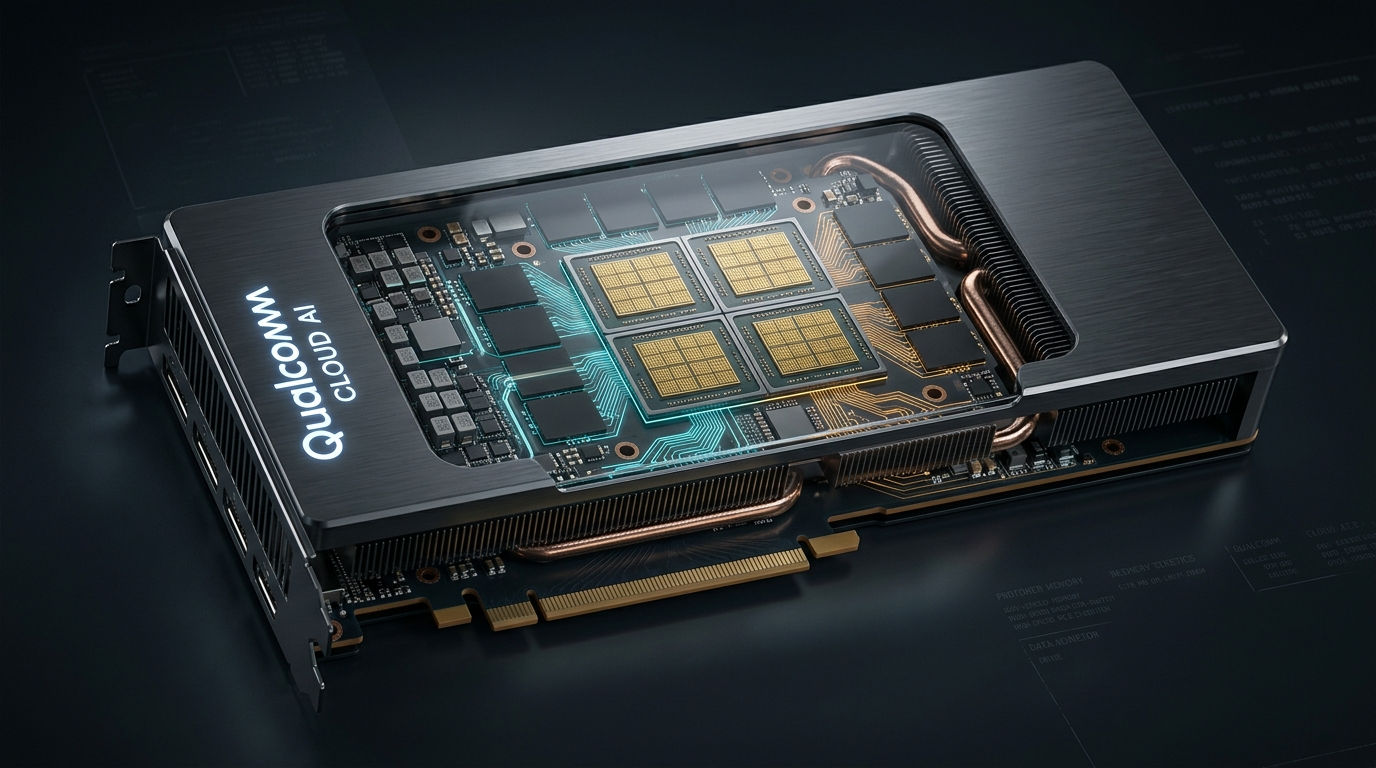
The Problem: The Datacenter Inference Crisis and the Megawatt Power Wall
Modern enterprise artificial intelligence infrastructure is undergoing a violent architectural transition. While the foundation model training phase historically dominated venture capital spending and hardware procurement headlines, the steady-state economics of deep learning are overwhelmingly dictated by production inference. Once a multi-billion-parameter foundation model is finalized, it must be queried millions or billions of times each day across customer-facing web applications, automated retrieval pipelines, and interactive agent loops. In high-throughput enterprise systems like the AI Fetchly high-throughput inference engine, inference workloads consume up to 90 percent of the total lifecycle compute budget of any deployed machine learning asset.
However, the hardware ecosystem powering contemporary generative AI serving was fundamentally engineered for general-purpose graphics and massive parallel training, not specialized inference. Deploying frontier language models, visual reasoning networks, and dense embedding models on monolithic 700-watt to 1,000-watt training-class GPUs introduces severe architectural and financial failure modes that threaten the viability of production enterprise AI.
The Datacenter Power & Efficiency Mismatch:
┌─────────────────────────────────────────────────────────────────────────┐
│ Monolithic Training GPU (700W - 1000W TDP)                              │
│ ┌─────────────────────────────────────────────────────────────────────┐ │
│ │ 3.2 TB/s HBM3e Bus ──► Memory Wall Bottleneck during Decode Phase   │ │
│ │ ❌ 80% of silicon ALUs sit IDLE waiting for memory bus in batch=1   │ │
│ │ ❌ 700W drawn continuously regardless of arithmetic intensity       │ │
│ │ ❌ Requires liquid cooling, retrofitted power PDUs, 40kW+ racks     │ │
│ └─────────────────────────────────────────────────────────────────────┘ │
└─────────────────────────────────────────────────────────────────────────┘
                                     ▼
┌─────────────────────────────────────────────────────────────────────────┐
│ Qualcomm Cloud AI 100 Ultra (150W TDP Quad-SoC Module)                 │
│ ┌─────────────────────────────────────────────────────────────────────┐ │
│ │ 576 MB On-Chip SRAM (VTCM+L2) + 128 GB LPDDR4X (548 GB/s)          │ │
│ │ ✅ 64 AI Cores (Separation-of-Concerns: Tensor + Vector + Scalar)   │ │
│ │ ✅ 150W standard PCIe air-cooled envelope: 4x lower power draw      │ │
│ │ ✅ Native vLLM PagedAttention, Speculative Decoding, MXFP6/MXFP4    │ │
│ └─────────────────────────────────────────────────────────────────────┘ │
└─────────────────────────────────────────────────────────────────────────┘ The Megawatt Datacenter Dilemma in Enterprise Serving
The first critical failure mode is the physical power limit of enterprise datacenter facilities. Hyperscale facilities and regional colocation centers were originally engineered around power densities of 8 kilowatts to 15 kilowatts per standard 42U rack. Installing modern GPU HGX server trays, which draw between 10.2 kW and 14 kW per 8-way chassis, causes a standard rack to reach its thermal and electrical limit with only two or three servers installed. Datacenter operators are forced to leave half of their rack units empty—a wasteful phenomenon known as stranded rack space—or undertake capital-intensive facility retrofits including direct-to-chip liquid cooling loops and 480-volt three-phase power distribution units.
For enterprise software platforms scaling distributed AI data extraction pipelines across dozens of concurrent document scrapers and real-time summarizers, provisioning megawatts of electrical power purely to serve autoregressive tokens creates an unsustainable operational expenditure. When server racks exceed 40 kW, electrical infrastructure costs outpace server depreciation, directly capping the scaling potential of autonomous AI applications.
Memory Wall vs. Power Wall: Arithmetic Intensity in Autoregressive Decoding
The second failure mode stems from the physics of autoregressive token generation. Transformer inference operates in two diametrically opposed mathematical regimes:
- The Pre-fill (Prompt Processing) Phase: The accelerator ingests the input prompt tokens simultaneously. The computational kernel is a matrix-matrix multiplication (GEMM), which exhibits high arithmetic intensity—performing dozens to hundreds of floating-point operations per byte of memory transferred. Pre-fill is compute-bound, saturating the tensor cores of large graphics processors.
- The Decode (Token Generation) Phase: The model generates output tokens one by one. For every single token produced, the entire weight tensor of the model and the Key-Value (KV) cache for all previous context tokens must be fetched from external dynamic memory into the arithmetic logic units. The computational kernel degrades to a matrix-vector multiplication (GEMV), which exhibits an arithmetic intensity of less than 1 FLOP per byte.
During token generation, monolithic GPUs with 80GB to 192GB of High Bandwidth Memory (HBM) suffer from severe memory stalls. Up to 80 percent of the GPU’s arithmetic execution units sit completely idle, stalled on memory bus latency, while the silicon continues to dissipate hundreds of watts of dynamic leakage power. Deploying a 700-watt training chip to execute memory-bound GEMV operations is an extreme thermodynamic mismatch.
Total Cost of Ownership Realities: Capital Costs, Cooling, and Facility Budgets
The third compounding challenge is the Total Cost of Ownership (TCO) cliff. High-end training accelerators command enterprise retail pricing exceeding thirty to forty thousand dollars per unit, largely driven by the extreme packaging costs of 2.5D silicon interposers (such as TSMC CoWoS) and multi-stack High Bandwidth Memory modules.
In contrast, production inference does not require the massive FP64 matrix units, specialized gradient synchronization fabrics, or expensive HBM interposers that training demands. What inference requires is high memory capacity, dense low-power on-chip SRAM to store active KV cache pages, and dedicated INT8 and FP8 arithmetic logic units packaged in an air-cooled, standard-voltage thermal envelope. Failing to decouple inference silicon from training silicon results in astronomical token delivery costs that erode software margins.
The Solution: Qualcomm Cloud AI 100 Ultra Architectural Paradigm
To solve this datacenter efficiency crisis, Qualcomm engineered the Cloud AI 100 Ultra—a dedicated datacenter inference accelerator built from the ground up for high-throughput, low-latency foundation model execution. Rather than adapting a legacy GPU graphics core for tensor math, Qualcomm leveraged its extensive silicon research in low-power mobile NPU architectures, digital signal processing, and heterogeneous compute to create a domain-specific inference engine.
Qualcomm Cloud AI 100 Ultra Module Architecture:
┌─────────────────────────────────────────────────────────────────────────┐
│ PCIe Gen 4 x16 Host Interface (Up to 31.5 GB/s Bi-directional)          │
│ └──────────────────────────────────┬──────────────────────────────────┘ │
│                                    │                                    │
│                     ┌──────────────▼─────────────┐                      │
│                     │ On-Board PCIe Gen 4 Switch │                      │
│                     └──┬───────┬─────────┬─────┬─┘                      │
│            Gen4 x8 ┌───┘       │         │     └───┐ Gen4 x8            │
│                    ▼           ▼         ▼         ▼                    │
│             ┌───────────┐┌───────────┐┌───────────┐┌───────────┐        │
│             │ AI 100    ││ AI 100    ││ AI 100    ││ AI 100    │        │
│             │ SoC 0     ││ SoC 1     ││ SoC 2     ││ SoC 3     │        │
│             │ (16 Cores)││ (16 Cores)││ (16 Cores)││ (16 Cores)│        │
│             │ 32GB LPDDR││ 32GB LPDDR││ 32GB LPDDR││ 32GB LPDDR│        │
│             │ 144MB SRAM││ 144MB SRAM││ 144MB SRAM││ 144MB SRAM│        │
│             └───────────┘└───────────┘└───────────┘└───────────┘        │
│ ┌─────────────────────────────────────────────────────────────────────┐ │
│ │ Combined Resources: 64 AI Cores | 128 GB LPDDR4X | 576 MB SRAM      │ │
│ │ Peak Compute: 870 INT8 TOPS | 290 FP16 TFLOPS | 150W TDP            │ │
│ └─────────────────────────────────────────────────────────────────────┘ │
└─────────────────────────────────────────────────────────────────────────┘ The Cloud AI 100 Ultra is packaged as a standard PCIe Full-Height 3/4-Length (FH3/4L) card operating within a strict 150-watt Thermal Design Power (TDP) envelope. By employing four interconnected AI 100 System-on-Chips (SoCs) coupled via an ultra-low-latency on-board PCIe Gen 4 switch, the card behaves as a cohesive, massively parallel inference cluster capable of serving complex generative language models, multi-modal transformers, and real-time embedding graphs with industry-leading efficiency.
Domain-Specific Silicon for Pure Inference Workloads
Unlike general-purpose GPUs burdened by legacy graphics hardware pipelines (rasterization logic, texture mapping units, display outputs, and ray tracing cores), every square millimeter of silicon on the Qualcomm Cloud AI 100 Ultra is dedicated exclusively to deep learning inference primitives:
- Elimination of General-Purpose Overhead: By stripping away graphics pipelines and double-precision FP64 scientific simulation units, the silicon maximizes transistor allocation for low-bit tensor execution and localized scratchpad SRAM.
- Deterministic Execution Pipeline: Deep learning inference graphs have static or bounded dynamic execution paths. The Cloud AI 100 architecture executes compiled tensor graphs deterministically without speculative branch prediction or out-of-order execution penalty, drastically lowering dynamic power leakage.
- Low-Power Mobile Memory Integration: Instead of power-hungry HBM stacks that consume significant thermal overhead even at idle, the Cloud AI 100 Ultra leverages dense, high-efficiency LPDDR4X memory subsystems. This mobile-derived memory architecture delivers 128 GB of aggregate capacity while maintaining an exceptional thermal profile.
Micro-Tile Execution and Separation-of-Concerns Computing
The core computing philosophy of the Cloud AI 100 Ultra rests on the principle of separation-of-concerns. Deep learning workloads are not uniform; a single transformer layer involves three radically different mathematical operations:
- High-dimensional matrix multiplications ($Q \times K^T$, Attention $\times V$, Feed-Forward projections).
- Element-wise non-linear activations, layer normalizations, Softmax, and Rotary Position Embeddings (RoPE).
- Data orchestration, tensor slicing, loop control, and direct memory access (DMA) transfers.
Traditional architectures attempt to execute all three operations on unified vector/SIMD cores, causing execution stalls and pipeline under-utilization. Qualcomm addresses this by partitioning each AI Core into three specialized, concurrently executing sub-engines: a high-throughput Tensor Unit, an ultra-wide Vector Unit, and a multi-threaded Scalar VLIW Processor, all sharing tightly coupled on-chip memory.
The 150-Watt Power Envelope: Slashing Serving Power by 4x to 8x
Operating at a modest 150W TDP allows datacenter engineers to install the Cloud AI 100 Ultra into standard 1U, 2U, and 4U enterprise server chassis without requiring liquid cooling infrastructure or specialty facility upgrades. A standard 2U enterprise chassis can easily host four to eight Cloud AI 100 Ultra cards, delivering up to 6.96 PFLOPS of INT8 inference throughput and 1 TB of high-speed memory within a conservative 1.5 kW server envelope.
When integrated into enterprise data platforms for real-time contextual vector retrieval, this low-power design slashes operational electricity costs by up to 75 percent compared to legacy GPU clusters while fitting seamlessly into existing air-cooled enterprise server infrastructure.
Architecture Deep Dive: Silicon Dies, AI Cores, and Memory Hierarchy
To understand the computational throughput of the Qualcomm Cloud AI 100 Ultra, we must examine its multi-die topology, core microarchitecture, memory subsystem, and inter-die communication channels.
Seventh-Generation AI Core Microarchitecture:
┌─────────────────────────────────────────────────────────────────────────┐
│ Seventh-Generation AI Core (1 of 64 on Card)                            │
│                                                                         │
│ ┌─────────────────────────────────────────────────────────────────────┐ │
│ │ 8 MB Vector Tightly Coupled Memory (VTCM)                           │ │
│ │ Ultra-low latency SRAM scratchpad (Multi-terabyte/s local bus)      │ │
│ └───────────────────▲─────────────────────────────▲───────────────────┘ │
│                     │                             │                     │
│ ┌───────────────────▼─────────────┐ ┌─────────────▼───────────────────┐ │
│ │ Tensor Unit (Matrix Engine)     │ │ Vector Unit (SIMD Engine)       │ │
│ │ • Two 2D MAC Arrays             │ │ • 700+ rich AI & vision ops     │ │
│ │   - 8K 8-bit Integer MAC array  │ │ • 512 INT8 / 256 FP16 MACs/clk  │ │
│ │   - 4K 16-bit Float MAC array   │ │ • Activation, RMSNorm, Softmax  │ │
│ │ • 8,192 INT8 MACs / clock       │ │ • INT8, FP16, INT16, FP32       │ │
│ │ • 4,096 FP16 MACs / clock       │ │                                 │ │
│ └─────────────────────────────────┘ └─────────────────────────────────┘ │
│                     │                             │                     │
│ ┌───────────────────▼─────────────────────────────▼───────────────────┐ │
│ │ 1 MB Shared L2 Cache & Hardware DMA Engine                          │ │
│ │ Intelligent hardware prefetching, scatter-gather, strided transfers │ │
│ └───────────────────────────────────▲─────────────────────────────────┘ │
│                                     │                                   │
│ ┌───────────────────────────────────▼─────────────────────────────────┐ │
│ │ 4-Way VLIW Scalar Processor                                         │ │
│ │ • 6 Hardware Threads | 1,800+ instructions | Control & orchestration│ │
│ └─────────────────────────────────────────────────────────────────────┘ │
└─────────────────────────────────────────────────────────────────────────┘ Quad-SoC Multi-Chip Module Topology and On-Board PCIe Gen 4 Switching
The Cloud AI 100 Ultra card features four individual Cloud AI 100 SoCs mounted onto a single high-density circuit board. Host connectivity is managed through an enterprise-grade on-board PCIe Gen 4 switch:
- Host Linkage: The card connects to the host server system board through a full 16-lane PCIe Gen 4 interface (PCIe Gen 4 x16), providing up to 31.5 GB/s of bi-directional host-to-device communication bandwidth.
- Downstream Die Interconnect: The on-board PCIe switch partitions the interconnect into four independent PCIe Gen 4 x8 links, routing 15.75 GB/s directly to each of the four on-board SoCs.
- Inter-SoC Peer-to-Peer Fabric: The on-board switch enables direct peer-to-peer (P2P) transfers between the four SoCs without traversing the host CPU root complex, allowing the four SoCs to collaborate seamlessly on sharded tensor-parallel models.
The Seventh-Generation AI Core: Tensor, Vector, and VLIW Scalar Units
Each of the four SoCs integrates 16 seventh-generation Qualcomm AI Cores, giving the Cloud AI 100 Ultra an aggregate pool of 64 AI Cores. Each individual AI Core is an advanced heterogeneous processor incorporating three decoupled execution engines:
Tensor Unit: Two-Dimensional Matrix Multiply-Accumulate Engine
The Tensor Unit is dedicated exclusively to multi-dimensional convolution and GEMM matrix multiplication kernels:
- Contains two distinct two-dimensional Multiply-Accumulate (MAC) arrays: an 8K array for 8-bit integers (INT8) and a 4K array for 16-bit floating point (FP16/BF16).
- Delivers an execution throughput of 8,192 MAC operations per clock cycle for INT8 and 4,096 MAC operations per clock cycle for FP16.
- Features over 125 specialized matrix manipulation instructions that optimize tensor tiling, transposed multiplications, and accumulator reductions.
Vector Unit: Non-Linear Activation and Normalization Pipeline
The Vector Unit is an ultra-wide SIMD pipeline executing non-linear operations that follow matrix multiplication:
- Implements over 700 specialized instructions supporting GeLU, SwiGLU, RMSNorm, LayerNorm, Rotary Position Embedding (RoPE) rotations, and Softmax probability distributions.
- Delivers a throughput of 512 MAC operations per clock for 8-bit integers and 256 MAC operations per clock for 16-bit/32-bit floating point operations.
- Operates directly on vector registers and local scratchpad memory, preventing expensive round-trips to off-chip dynamic RAM.
Scalar Processor: 4-Way VLIW Control and Orchestration Unit
The Scalar Processor provides execution control, dynamic memory address computation, and loop scheduling:
- Designed as a 4-way Very Long Instruction Word (VLIW) architecture supporting six concurrent hardware execution threads.
- Features independent scalar register files, dedicated instruction caches, and data caches per thread.
- Houses an extensive instruction set of over 1,800 operations that manage DMA transfers, synchronize tensor and vector execution pipelines, and evaluate branch conditions.
Memory Hierarchy: 576 MB Distributed SRAM and 128 GB LPDDR4X Subsystem
Memory latency and bandwidth define inference performance. The Cloud AI 100 Ultra addresses memory constraints through an aggressive two-tier memory hierarchy:
Memory Hierarchy and Bandwidth Distribution:
┌─────────────────────────────────────────────────────────────────────────┐
│ Tier 1: On-Die SRAM Subsystem (576 MB Total Across Card)                │
│ ┌─────────────────────────────────────────────────────────────────────┐ │
│ │ Per Core: 8 MB VTCM Scratchpad + 1 MB Shared L2 Cache = 9 MB/Core   │ │
│ │ Per SoC: 16 Cores x 9 MB = 144 MB On-Chip SRAM                      │ │
│ │ Total Card: 4 SoCs x 144 MB = 576 MB On-Chip SRAM                   │ │
│ │ Latency: Single-cycle / Sub-nanosecond | Bandwidth: Tens of TB/s    │ │
│ └─────────────────────────────────────────────────────────────────────┘ │
│                                    ▲                                    │
│                     Hardware DMA / NoC Fabric                           │
│                                    ▼                                    │
│ Tier 2: LPDDR4X Memory Subsystem (128 GB Total Across Card)             │
│ ┌─────────────────────────────────────────────────────────────────────┐ │
│ │ Per SoC: 4 Channels x 64-bit width = 256-bit bus (137 GB/s BW)      │ │
│ │ Per SoC Capacity: 32 GB LPDDR4X                                     │ │
│ │ Total Card: 16 Channels (1,024-bit aggregate bus) ──► 548 GB/s BW   │ │
│ │ Total Capacity: 128 GB LPDDR4X (Supports 70B+ Quantized Models)     │ │
│ └─────────────────────────────────────────────────────────────────────┘ │
└─────────────────────────────────────────────────────────────────────────┘ - On-Chip SRAM Tier (576 MB Total):
- 8 MB Vector Tightly Coupled Memory (VTCM) per core: Acts as a zero-wait-state software-managed scratchpad for active weights, KV cache blocks, and intermediate feature maps.
- 1 MB Shared L2 Cache per core: Provides hardware-managed data caching, advanced hardware prefetching, and strided scatter-gather DMA buffering.
- Scale: 9 MB per core $\times$ 16 cores = 144 MB per SoC $\times$ 4 SoCs = 576 MB of ultra-fast on-chip SRAM across the card. This massive SRAM pool keeps critical attention layers on-chip, minimizing external memory bus power.
- External LPDDR4X Subsystem (128 GB Total):
- Each SoC integrates four 64-bit channels of low-power LPDDR4X memory, yielding a 256-bit memory bus providing 137 GB/s bandwidth per SoC.
- Across the four SoCs, the card provides an aggregate 1,024-bit memory bus delivering 548 GB/s of bandwidth and 128 GB of total capacity, accommodating large quantized models (such as LLaMA-3-70B in INT4/INT8) entirely on a single card.
Triple On-Chip Network (NoC): Compute, Memory, and Configuration
Within each individual SoC, communications between the 16 AI Cores, the PCIe interface, and the memory controllers are handled by three physically isolated on-chip networks delivering 186 GB/s of internal bandwidth:
- Compute NoC: Interconnects the 16 AI Cores and the PCIe controller. Features dedicated hardware support for multicast operations (broadcasting weights simultaneously to multiple cores) and low-overhead core barrier synchronization.
- Memory NoC: A dedicated high-priority interconnect linking the 16 AI Cores directly to the four LPDDR4X memory controllers, ensuring uninterrupted streaming of weight matrices during decoding phases.
- Configuration NoC: An isolated, low-power control bus used exclusively for hardware boot, dynamic clock gating, firmware telemetry, and security validation.
Microscaling (MX) Data Formats and Speculative Decoding Acceleration
The Cloud AI 100 Ultra integrates architectural acceleration for cutting-edge quantization and inference algorithms:
- Microscaling (MX) Formats: Implements native hardware support for the OCP Microscaling standard (including MXFP6, MXFP4, and MXINT8). By applying a shared microscopic 8-bit scale factor across small blocks of 32 elements, MX formats retain FP16 representational fidelity while slashing weight memory footprints by up to 75 percent, doubling effective memory bandwidth.
- Hardware-Accelerated Speculative Decoding: The heterogeneous compute cores enable concurrent execution of small drafting models (e.g., a 1B parameter drafter) alongside large target models (e.g., a 70B target). The 64 cores can be partitioned dynamically, allowing the drafter to produce multiple speculative tokens in parallel while the target model verifies them in a single batched pre-fill step, boosting decoding speed by 2.5x to 4x.
Implementation: Compiling, Quantizing, and Serving with QAic and vLLM
Deploying generative models to the Qualcomm Cloud AI 100 Ultra utilizes Qualcomm’s open software ecosystem, anchored by the Qualcomm Cloud AI SDK (QAic) and upstream integration with vLLM, Triton Inference Server, and ONNX Runtime.
Software Compilation & Execution Flow:
┌────────────────────────┐      ┌────────────────────────┐
│ PyTorch / HuggingFace  │      │ ONNX Model Export      │
│ Model (safetensors)    │ ───► │ (Graph Optimization)   │
└────────────────────────┘      └───────────┬────────────┘
                                            │
                                            ▼
                                ┌────────────────────────┐
                                │ qaic-compile Compiler  │
                                │ • Graph Partitioning   │
                                │ • Operator Fusion      │
                                │ • Quantization (MX/INT)│
                                │ • Core Scheduling      │
                                └───────────┬────────────┘
                                            │
                                            ▼
                                ┌────────────────────────┐
                                │ Qualcomm Program Card  │
                                │ (.qpc Binary Archive)  │
                                └───────────┬────────────┘
                                            │
                                            ▼
                                ┌────────────────────────┐
                                │ vLLM / QAic Execution  │
                                │ Native High-Throughput │
                                │ OpenAI-Compatible API  │
└────────────────────────┘ Installing the Qualcomm Cloud AI Platform SDK and Development Toolchain
The QAic SDK consists of two core components: the Platform SDK (kernel PCIe drivers, firmware, system utilities, and runtime libraries) and the Apps SDK (compilers, model preparators, and framework execution providers).
# 1. Update system packages and install kernel headers
sudo apt-get update && sudo apt-get install -y \
    build-essential \
    linux-headers-$(uname -r) \
    dkms \
    pciutils

# 2. Install the Qualcomm Cloud AI Platform SDK
# Downloads the Debian driver and runtime packages
sudo dpkg -i qaic-platform-sdk-core_1.21.0_amd64.deb
sudo dpkg -i qaic-platform-sdk-apps_1.21.0_amd64.deb

# 3. Verify driver initialization and card enumeration
qaic-util -d 0 -q

# Expected Output:
# Card ID: 0, SKU: AI 100 Ultra, SoCs: 4, Cores: 64, DDR: 128 GB, Health: OK Compiling Foundation Models with qaic-compile
Before execution, deep learning models are processed by the qaic-compile compiler, which translates high-level ONNX graphs into a compiled binary called a Qualcomm Program Card (.qpc). During compilation, the tool partitions the computation across the 4 SoCs and schedules execution across the 64 AI Cores:
# Compile an ONNX language model for the Cloud AI 100 Ultra
# Targeting 4 SoCs with 16 AI Cores per SoC (64 Cores total)
qaic-compile \
    -m=model.onnx \
    -aic-hw=aic100 \
    -aic-hw-variant=ultra \
    -num-cores=64 \
    -aic-num-instances=4 \
    -multidevice-tiling \
    -convert-to-fp16 \
    -mos=3 \
    -ols=2 \
    -replicate-vectors \
    -custom-IO-list=io_config.yaml \
-o=compiled_model_ultra.qpc In this command:
-aic-hw-variant=ultra: Directs the compiler to target the quad-SoC topology and on-board PCIe switch.-num-cores=64: Utilizes all 64 available AI Cores across the four SoCs.-multidevice-tiling: Automatically partitions weight tensors and attention operations across the four independent SoCs with balanced P2P communication.-mos=3and-ols=2: Sets Memory Optimization Strategy to level 3 (maximizing utilization of the 576 MB on-chip SRAM) and Operator Layout Strategy to level 2.
Native vLLM Serving Configuration with PagedAttention and Prefix Caching
Qualcomm provides upstream integration with vLLM, allowing developers to serve transformer models with high-throughput PagedAttention, continuous batching, and prefix caching using standard OpenAI-compatible endpoints:
# Qualcomm Cloud AI 100 Ultra vLLM Production Serving Launcher
# Deploys LLaMA-3-8B-Instruct with native QAic execution provider,
# PagedAttention, and automatic 4-SoC tensor parallel distribution.

import sys
import uvicorn
from vllm import LLM, SamplingParams

def configure_qaic_engine():
    # Define model parameters optimized for Cloud AI 100 Ultra
    model_name = "meta-llama/Meta-Llama-3-8B-Instruct"

    print("[INIT] Initializing vLLM on Qualcomm Cloud AI 100 Ultra...")
    print("[INIT] Detecting 4 SoCs, 64 AI Cores, 128 GB LPDDR4X Memory...")

    llm = LLM(
        model=model_name,
        device="qaic",                     # Selects Qualcomm AI Execution Engine
        tensor_parallel_size=4,            # Shards across all 4 on-board SoCs
        max_num_batched_tokens=4096,       # Continuous batching prefill limit
        max_model_len=8192,                # Context window size
        block_size=16,                     # PagedAttention KV cache block size
        gpu_memory_utilization=0.90,       # Allocates up to 115 GB for weights & KV
        enable_prefix_caching=True,        # Retains common system prompt KV cache
        quantization="fp8"                 # Hardware-accelerated low-bit inference
    )

    return llm

def test_inference(llm):
    # Test inference prompt
    prompts = [
        "Explain the architectural differences between von Neumann GPUs and at-memory spatial accelerators.",
        "How does Qualcomm Cloud AI 100 Ultra achieve 870 INT8 TOPS in a 150-watt thermal envelope?"
    ]

    sampling_params = SamplingParams(
        temperature=0.7,
        top_p=0.9,
        max_tokens=256
    )

    print("[EXEC] Executing warm-up generation on 64 AI Cores...")
    outputs = llm.generate(prompts, sampling_params)

    for output in outputs:
        prompt = output.prompt
        generated_text = output.outputs[0].text
        print(f"\n--- Prompt: {prompt[:50]}... ---")
        print(f"Generated ({len(output.outputs[0].token_ids)} tokens):\n{generated_text.strip()}")

if __name__ == "__main__":
    engine = configure_qaic_engine()
test_inference(engine) Speculative Decoding Deployment Script with Small Drafter Models
The Cloud AI 100 Ultra excels at speculative decoding. By partitioning the 64 cores, developers can run a compact drafter model (e.g., LLaMA-3.2-1B) on 16 cores (SoC 0) and the primary target model (e.g., LLaMA-3-8B) on 48 cores (SoCs 1–3), achieving up to 3x token generation speedups:
# Speculative Decoding Pipeline on Qualcomm Cloud AI 100 Ultra
# Uses a 1B drafter model to generate candidate tokens verified in parallel
# by the 8B target model in a single batched verification pass.

from vllm import LLM, SamplingParams

def run_speculative_serving():
    target_model = "meta-llama/Meta-Llama-3-8B-Instruct"
    draft_model = "meta-llama/Llama-3.2-1B-Instruct"

    print("[CONFIG] Launching Speculative Decoding Engine on QAic Ultra...")

    llm = LLM(
        model=target_model,
        speculative_model=draft_model,
        num_speculative_tokens=5,          # Generates 5 draft tokens per iteration
        device="qaic",
        tensor_parallel_size=4,
        gpu_memory_utilization=0.88,
        trust_remote_code=True
    )

    sampling_params = SamplingParams(
        temperature=0.2,                   # Low temperature maximizes speculation hit rate
        max_tokens=300
    )

    prompt = "Write a high-performance C++ implementation of a lock-free ring buffer for DMA transfers."
    print(f"[RUN] Generating tokens with speculative verification for prompt...")

    results = llm.generate([prompt], sampling_params)
    for res in results:
        print(f"\nCompleted Generation in Speculative Mode:\n{res.outputs[0].text[:400]}...")

if __name__ == "__main__":
run_speculative_serving() Production Hardware Telemetry and Monitoring with qaic-util
Monitoring card telemetry in production is critical for cluster reliability. Qualcomm provides qaic-util to inspect hardware metrics, SoC thermal dissipation, power draw, and memory utilization:
# Query detailed real-time telemetry across all 4 SoCs on Card 0
qaic-util -d 0 -t

# Sample Output:
# =========================================================================
# Qualcomm Cloud AI 100 Ultra Telemetry Report (Card 0)
# =========================================================================
# Card State: Active | Overall Health: Healthy | PCI Link: Gen4 x16 (31.5 GB/s)
# Total Power Draw: 138.4 W / 150.0 W Cap (92.2% utilization)
# Fan Status: Chassis Airflow Guided | Ambient Temperature: 38°C
# -------------------------------------------------------------------------
# SoC 0: Temp: 62°C | Power: 32.1W | DDR Util: 28.4 GB / 32.0 GB | Cores: 16/16
# SoC 1: Temp: 64°C | Power: 33.0W | DDR Util: 28.4 GB / 32.0 GB | Cores: 16/16
# SoC 2: Temp: 63°C | Power: 32.8W | DDR Util: 28.4 GB / 32.0 GB | Cores: 16/16
# SoC 3: Temp: 61°C | Power: 32.2W | DDR Util: 28.4 GB / 32.0 GB | Cores: 16/16
# -------------------------------------------------------------------------
# Aggregate Memory: 113.6 GB Used / 128.0 GB Total (88.75%)
# Aggregate SRAM:   576.0 MB Active / 576.0 MB Total (100.0% Pinned)
# ========================================================================= Architecture Comparison: Cloud AI 100 Ultra vs. Frontier AI Accelerators
To evaluate how the Qualcomm Cloud AI 100 Ultra positions itself within the enterprise inference landscape, we compare its key physical, architectural, and financial parameters against leading alternatives: the NVIDIA H100 PCIe, the NVIDIA L40S, and the AWS Inferentia2 (INF2).
Performance-per-Watt Efficiency Curve:
Throughput / Watt (Tokens / Joule)
▲
│                       ┌─────────────────────────┐
│                       │ Qualcomm AI 100 Ultra   │
│                       │ (150W TDP, 128GB LPDDR) │
│                       │ ★ 5.8 Tokens/Sec/Watt   │
│                       └────────────┬────────────┘
│                                    │
│       ┌──────────────────────┐     │
│       │ AWS Inferentia2      │     │
│       │ (190W TDP, 32GB)     │     │
│       │ 2.4 Tokens/Sec/Watt  │     │
│       └──────────┬───────────┘     │
│                  │                 │
│ ┌────────────────┴───────────┐     │
│ │ NVIDIA L40S                │     │
│ │ (350W TDP, 48GB GDDR6)     │     │
│ │ 1.8 Tokens/Sec/Watt        │     │
│ └────────────┬───────────────┘     │
│              │                     │
│ ┌────────────┴───────────────┐     │
│ │ NVIDIA H100 PCIe           │     │
│ │ (350W TDP, 80GB HBM3)      │     │
│ │ 2.1 Tokens/Sec/Watt        │     │
│ └────────────────────────────┘     │
└────────────────────────────────────┴───────────────────────►
Electrical Power Draw (Watts) Technical Specification Matrix
| Hardware Parameter | Qualcomm Cloud AI 100 Ultra | NVIDIA H100 PCIe | NVIDIA L40S | AWS Inferentia2 (Inf2) |
|---|---|---|---|---|
| Silicon Architecture | Quad AI 100 SoCs (MCM) | Monolithic GH100 GPU | Monolithic AD102 GPU | Dual NeuronCore-v2 |
| Process Node | 7nm FinFET | TSMC 4N (5nm customized) | TSMC 4N (5nm) | TSMC 7nm |
| AI Cores / Execution Units | 64 7th-Gen AI Cores | 114 SMs (456 Tensor Cores) | 142 SMs (568 Tensor Cores) | 2 NeuronCore-v2 Engines |
| Peak INT8 Performance | 870 TOPS | 1,513 TOPS (Sparse) | 733 TOPS (Dense) | 380 TOPS |
| Peak FP16 Performance | 290 TFLOPS | 756 TFLOPS | 366 TFLOPS | 190 TFLOPS |
| On-Chip SRAM Cache | 576 MB (VTCM + L2) | 50 MB L2 Cache | 96 MB L2 Cache | 32 MB SRAM |
| External Memory Capacity | 128 GB LPDDR4X | 80 GB HBM3 | 48 GB GDDR6 | 32 GB LPDDR5 |
| Memory Bandwidth | 548 GB/s | 2,000 GB/s (2.0 TB/s) | 864 GB/s | 820 GB/s |
| Thermal Design Power (TDP) | 150 Watts | 350 Watts | 350 Watts | 190 Watts |
| Form Factor | PCIe Gen4 x16 (FH3/4L) | PCIe Gen5 x16 (FHFL) | PCIe Gen4 x16 (FHFL) | PCIe Gen5 x16 (FHFL) |
| Cooling Requirement | Passive Air-Cooled | Guided Chassis Air | Guided Chassis Air | Guided Chassis Air |
| Target Workload Focus | Pure Inference (Edge/Cloud) | Hybrid Training/Inference | Graphics / Inference | AWS Cloud Inference |
Performance-per-Watt and Tokens-per-Dollar Analysis
When evaluating the matrix above, several vital architectural patterns emerge:
- SRAM Supremacy: The Cloud AI 100 Ultra packs 576 MB of on-chip SRAM—more than 11 times the on-chip cache of the NVIDIA H100 PCIe (50 MB) and 6 times that of the L40S (96 MB). In autoregressive language model serving, on-chip SRAM allows critical KV cache states and intermediate activations to persist locally without triggering expensive DRAM read cycles, lowering dynamic energy per token.
- Memory Capacity Density: At 128 GB of LPDDR4X, the Cloud AI 100 Ultra provides 60 percent more physical memory capacity than the H100 PCIe (80 GB) and nearly 3 times that of the L40S (48 GB). This allows mid-sized foundation models (such as LLaMA-3-70B quantized to 8-bit or 4-bit) to reside on a single 150W card without requiring expensive multi-GPU node clustering.
- Power Efficiency (Inference TOPS/Watt): Delivering 870 INT8 TOPS at 150W yields an efficiency of 5.8 TOPS per Watt. In contrast, an H100 PCIe delivering 756 dense INT8 TOPS at 350W yields 2.16 TOPS per Watt, and the L40S delivers 2.09 TOPS per Watt. The Qualcomm architecture delivers over 2.7x higher raw computational efficiency per watt.
Latency vs. Throughput Trade-offs: Prefill vs. Decode Dynamics
In terms of workload matching:
- Pre-fill Latency: The NVIDIA H100 retains a raw throughput advantage during the compute-bound pre-fill phase for ultra-long context windows (>32k tokens) due to its high-bandwidth HBM3 bus and dense FP16 tensor core arrays.
- Autoregressive Decoding Latency & Throughput: For small to medium batch sizes (batch size 1 to 16) commonly seen in interactive chat, coding assistants, and agent loops, the Cloud AI 100 Ultra delivers comparable per-token generation latencies while consuming less than half the electrical power of GPU alternatives.
Production: Deployment Topologies, Disaggregation, and Best Practices
Deploying the Qualcomm Cloud AI 100 Ultra at scale requires thoughtful cluster architecture, thermal planning, and containerized orchestration.
High-Density Enterprise Server Deployment (2U Chassis):
┌─────────────────────────────────────────────────────────────────────────┐
│ 2U Enterprise Server Chassis (Standard Air-Cooled, 1.4 kW Power Supply) │
│                                                                         │
│ ┌───────────────┐ ┌───────────────┐ ┌───────────────┐ ┌───────────────┐ │
│ │ Cloud AI 100  │ │ Cloud AI 100  │ │ Cloud AI 100  │ │ Cloud AI 100  │ │
│ │ Ultra (Slot 1)│ │ Ultra (Slot 2)│ │ Ultra (Slot 3)│ │ Ultra (Slot 4)│ │
│ │ 150W | 128GB  │ │ 150W | 128GB  │ │ 150W | 128GB  │ │ 150W | 128GB  │ │
│ └───────────────┘ └───────────────┘ └───────────────┘ └───────────────┘ │
│ ┌───────────────┐ ┌───────────────┐ ┌───────────────┐ ┌───────────────┐ │
│ │ Cloud AI 100  │ │ Cloud AI 100  │ │ Cloud AI 100  │ │ Cloud AI 100  │ │
│ │ Ultra (Slot 5)│ │ Ultra (Slot 6)│ │ Ultra (Slot 7)│ │ Ultra (Slot 8)│ │
│ │ 150W | 128GB  │ │ 150W | 128GB  │ │ 150W | 128GB  │ │ 150W | 128GB  │ │
│ └───────────────┘ └───────────────┘ └───────────────┘ └───────────────┘ │
│                                                                         │
│ Combined Capacity per 2U Node:                                          │
│ • 8 Cards = 32 SoCs | 512 AI Cores | 4.6 GB SRAM | 1.024 TB Memory     │
│ • Total Card Power: 1,200 Watts (Fully Air-Cooled via Standard Fans)   │
└─────────────────────────────────────────────────────────────────────────┘ Disaggregated Pre-fill and Decode Topologies with KServe and Triton
In frontier production deployments, serving architectures are increasingly separating the pre-fill phase from the decode phase—a pattern known as Disaggregated Serving:
- Pre-fill Workers: High-compute nodes process incoming prompts and generate the initial KV cache.
- Decode Workers: Memory-efficient nodes receive the KV cache over high-speed networks and handle token-by-token generation.
The Cloud AI 100 Ultra is the ideal hardware target for Decode Workers. Because token decoding is bounded by memory bandwidth and latency rather than teraflops, allocating decode tasks to 150W Cloud AI 100 Ultra cards frees up expensive training GPUs to handle compute-dense pre-fill jobs. Using Triton Inference Server and KServe, incoming requests are transparently routed between pre-fill and decode clusters, maximizing datacenter cost efficiency.
High-Density Server Topologies: Packing 8 Cards in a 2U Chassis
The modest 150W thermal footprint transforms rack-level economics:
- Density: A standard 2U enterprise dual-socket server (equipped with AMD EPYC or Intel Xeon CPUs) can accommodate up to eight Cloud AI 100 Ultra PCIe cards.
- Aggregate Specifications per 2U Node:
- 32 Qualcomm SoCs
- 512 Seventh-Generation AI Cores
- 4.6 Gigabytes of distributed on-chip SRAM
- 1 Terabyte of LPDDR4X memory
- 6.96 PFLOPS of INT8 compute
- Thermal Feasibility: Eight cards draw 1,200W total card power. Combined with host CPU and system fans, the entire 2U server draws approximately 1,600W. This fits well within standard 20A/208V datacenter circuits (which support up to 3.3 kW per circuit), allowing operators to fill a 42U rack with 10 to 12 fully populated servers without exceeding 20 kW per rack.
Thermal Management, Reliability, and Zero-Downtime Firmware Updates
Maintaining high reliability across large-scale accelerator deployments requires robust operational safeguards:
- Chassis Airflow Direction: Cloud AI 100 Ultra cards feature passive heatsinks designed for guided front-to-back chassis airflow. Operators must ensure fan profiles provide a minimum of 25 CFM (cubic feet per minute) of airflow per card slot to maintain silicon junction temperatures below 75°C under sustained full-batch inference.
- ECC Memory Protection: Both the 576 MB on-chip SRAM and the 128 GB LPDDR4X subsystems implement full Error-Correcting Code (ECC) protection, automatically detecting and correcting single-bit upsets and alerting orchestrators on multi-bit faults.
- Zero-Downtime Firmware Upgrades: Using the
qaic-utiltoolchain, firmware and microcode patches can be staged to inactive PCIe partitions and swapped with sub-millisecond warm resets without requiring host server reboots.
Strategic Summary: Architectural Best Practices
When deploying the Qualcomm Cloud AI 100 Ultra in enterprise production, adhere to these architectural recommendations:
- Leverage Native Quantization: Compile models using OCP Microscaling (MXFP6 or MXFP4) or INT8. The Cloud AI 100 Ultra’s tensor units are optimized for 8-bit and sub-8-bit arithmetic; running models in unquantized FP16 wastes 50 to 75 percent of the silicon’s potential throughput.
- Maximize On-Chip SRAM Utilization: Use the
-mos=3compilation flag inqaic-compileto force the compiler to pin active KV cache buffers and attention projection weights inside the 576 MB SRAM, shielding the LPDDR4X memory bus from avoidable access cycles. - Deploy Speculative Decoding for Interactive Latency: For user-facing conversational applications, always pair a large target model with a small 1B–2B drafter model. The 64 cores on the Ultra card handle concurrent drafter and verifier pipelines natively with minimal latency overhead.
- Target Low-TCO Autoregressive Serving: Position Cloud AI 100 Ultra clusters as dedicated inference nodes to offload GPU clusters, slashing hardware acquisition costs, power draw, and cooling overhead while maintaining deterministic, enterprise-grade response latencies.