MemryX MX3: Compute-at-Memory Edge AI Architecture Guide
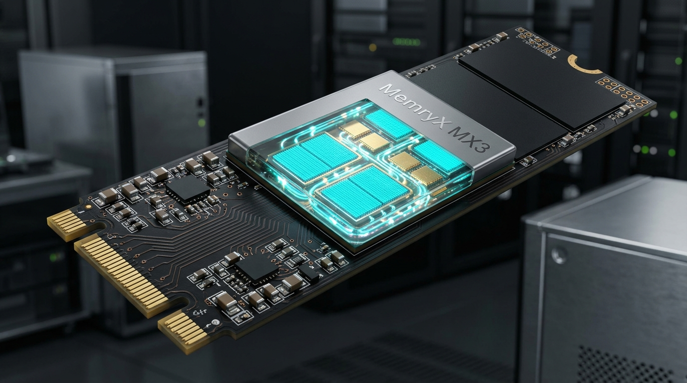
The Problem: The Edge AI Deployment Trap, Host CPU Friction, and Compiler Latency
The rapid expansion of artificial intelligence into enterprise edge devices—spanning industrial smart cameras, automated quality inspection systems, retail analytics, and autonomous robotics—has revealed severe systemic bottlenecks in contemporary edge acceleration silicon. While centralized cloud datacenters operate under massive multi-kilowatt power budgets and rely on vast software engineering teams, edge computing environments are constrained by strict physical, thermal, and operational limits.
In high-throughput enterprise platforms like the AI Fetchly high-throughput inference engine, executing real-time object tracking, multi-camera classification, and localized document feature extraction requires edge processors that operate with sub-50-millisecond response times. However, deploying modern deep learning models onto first-generation edge neural processing units (NPUs) and embedded GPUs introduces three crippling friction points that stall commercial adoption.
Traditional Edge NPU Friction vs. MemryX Compute-at-Memory Architecture:
┌─────────────────────────────────────────────────────────────────────────┐
│ Traditional Edge NPU / Embedded GPU:                                    │
│ ┌─────────────────────────────────────────────────────────────────────┐ │
│ │ Complex Compiler Toolchains ──► Hours of Quantization & Tuning       │ │
│ │ Heavy Host CPU Interrupts ──► Host CPU Spikes to 80% Utilization    │ │
│ │ Packetized NoC Routing & External DDR ──► High Dynamic Power (>10W) │ │
│ └─────────────────────────────────────────────────────────────────────┘ │
└─────────────────────────────────────────────────────────────────────────┘
                                     ▼
┌─────────────────────────────────────────────────────────────────────────┐
│ MemryX MX3 Compute-at-Memory Dataflow Architecture:                     │
│ ┌─────────────────────────────────────────────────────────────────────┐ │
│ │ Memory as the Sole Interconnect ──► Zero Control Plane or NoC       │ │
│ │ One-Click Model Compilation in Seconds ──► Native PyTorch / ONNX    │ │
│ │ Autonomous Streaming ──► Zero Host CPU Loading | Sub-Watt Power     │ │
│ │ Seamless Multi-Chip Cascade ──► Up to 16 Chips as One Logical Unit  │ │
│ └─────────────────────────────────────────────────────────────────────┘ │
└─────────────────────────────────────────────────────────────────────────┘ The Software Friction in Edge AI: Hours of Compilation and Fragile Quantization
The single greatest hidden cost in edge artificial intelligence is software complexity. For most commercial edge NPUs, compiling a pre-trained neural network is a grueling multi-day ordeal:
- Extensive Compiler Tuning: Developers must navigate proprietary, highly fragile compiler toolchains that require manual layer partitioning, custom operator rewrites, and hardware-specific tiling annotations.
- Complex Calibration Loops: Post-Training Quantization (PTQ) on traditional edge silicon often causes unpredictable accuracy collapse, forcing engineers into hardware-in-the-loop calibration cycles and model retraining.
- Slow Turnaround Cycles: A compiler that takes thirty minutes to two hours to compile a single model binary paralyzes agile deployment pipelines, preventing rapid iteration across computer vision models.
When enterprise data pipelines, such as distributed AI data extraction pipelines ingesting thousands of visual document formats, attempt to roll out updated vision models to edge nodes, slow compilation pipelines create significant operational friction.
The Hidden Host Overhead: How Traditional NPUs Steal Host CPU Cycles
A widespread deception in edge AI hardware benchmarking is the concept of standalone accelerator performance. While an edge accelerator may boast high peak tera-operations per second (TOPS), operating that chip in a real-world system frequently overwhelms the host processor:
- Interrupt and Memory Marshalling Storms: Traditional NPUs execute layer-by-layer. At every layer boundary, the accelerator generates hardware interrupts, forcing the host CPU to manage direct memory access (DMA) buffers, reformat intermediate tensors, and schedule the next kernel.
- Host CPU Saturation: In multi-stream video surveillance systems, host CPUs (such as Intel Core i5/i7 or ARM Cortex-A processors) spend up to 70 to 80 percent of their processing cycles merely feeding data to the NPU. This prevents the host from running essential application logic, databases, or web servers, forcing system builders to purchase expensive, power-hungry host CPUs.
Memory as a Traffic Jam: Control Planes, Packet Arbitration, and Thermal Degradation
In conventional edge accelerators, memory is separated from compute logic by long interconnect buses or complex packetized Networks-on-Chip (NoCs). Every tensor transfer requires arbitration, packet serialization, flow control headers, and address decoding:
- The NoC Energy Tax: Up to 30 percent of total chip silicon area and dynamic power is wasted on routers, buffers, and packet arbiters that perform no mathematical work.
- Thermal Saturation: Moving intermediate activation tensors between processing elements and centralized caches dissipates substantial heat, causing compact M.2 cards to reach 85°C and thermal throttle under continuous inference loads.
The Solution: MemryX MX3 and the Compute-at-Memory Dataflow Paradigm
To eliminate software friction, host CPU dependency, and interconnect power waste, Ann Arbor-based semiconductor pioneer MemryX Inc.—founded by University of Michigan Professor Dr. Wei Lu (IEEE Fellow and renowned authority on neuromorphic memory systems)—engineered the MemryX MX3 Edge AI Accelerator.
Compute-at-Memory Dataflow Engine Flow:
┌─────────────────────────────────────────────────────────────────────────┐
│ Input Data Stream (Camera Video Frames / Sensor Telemetry)              │
│ └──────────────────────────────────┬──────────────────────────────────┘ │
│                                    │ Continuous FIFO Push               │
│ ┌──────────────────────────────────▼──────────────────────────────────┐ │
│ │ Layer 0: Compute-at-Memory Bank (Weights Pinned in SRAM)            │ │
│ │ • Instantaneous Multiply-Accumulate Execution                       │ │
│ └──────────────────────────────────┬──────────────────────────────────┘ │
│                                    │ Direct Memory Handoff (No NoC!)    │
│ ┌──────────────────────────────────▼──────────────────────────────────┐ │
│ │ Layer 1: Compute-at-Memory Bank (Weights Pinned in SRAM)            │ │
│ │ • Instantaneous Multiply-Accumulate Execution                       │ │
│ └──────────────────────────────────┬──────────────────────────────────┘ │
│                                    │ Direct Memory Handoff (No NoC!)    │
│ ┌──────────────────────────────────▼──────────────────────────────────┐ │
│ │ Layer N: Final Output Classification / Bounding Box Stream          │ │
│ └─────────────────────────────────────────────────────────────────────┘ │
└─────────────────────────────────────────────────────────────────────────┘ The MemryX MX3 is an ultra-low-power, high-efficiency AI accelerator built upon a radical architectural premise: Compute-at-Memory with memory as the sole interconnect. By co-locating digital arithmetic logic directly inside distributed static RAM (SRAM) banks and allowing data to stream continuously through the memory hierarchy like water through a pipe, the MX3 achieves up to 6 TFLOPS and 12 TOPS of computing throughput at sub-watt typical power dissipation.
The Concept of Memory as the Sole Interconnect
In traditional computer engineering, memory and interconnect are separate entities: compute engines process data, and a Network-on-Chip or bus routes data to memory. MemryX completely discards the control plane and on-chip routing network:
- Memory Is the Wire: Memory buffers serve as the direct physical interface between adjacent compute engines. When processing node $N$ completes its layer calculation, it writes its output directly into the memory bank of processing node $N+1$.
- Zero Global Arbitration: There are no packet headers, no route discovery tables, and no bus arbiters. Data movement is driven entirely by local memory read/write availability, eliminating millions of transistors of unnecessary overhead.
- Deterministic Execution Flow: Because data flows along a fixed physical graph established at model compilation, execution timing is perfectly deterministic, with zero contention or variable latency spikes.
Streaming Dataflow: Asynchronous Pipelining from Layer to Layer
The MX3 operates on a pure streaming dataflow model:
- Layer Pipelining: Model layers are distributed spatially across the chip’s internal compute-at-memory banks.
- Continuous Frame Ingestion: As new video frames or sensor vectors enter the chip, they stream through the pipeline in continuous waves. While layer 5 processes frame $K$, layer 4 is simultaneously processing frame $K+1$, and layer 3 is processing frame $K+2$.
- Extreme Memory Reuse: Model weights remain stationary inside their assigned compute-at-memory banks throughout the entire application lifecycle. Intermediate activation tensors are consumed immediately by the adjacent downstream bank, completely eliminating external dynamic RAM (DRAM) read/write cycles.
The Sub-Watt Performance Profile: 6 TFLOPS at Sub-1W Power
By combining compute-at-memory proximity with dataflow streaming, the MX3 delivers unprecedented energy efficiency:
- True Sub-Watt Operation: Consumes between 0.5W and 1.5W under full-speed production workloads, enabling fanless, sealed enclosure deployment across edge appliances.
- Floating-Point and Integer Versatility: Delivers up to 6 TFLOPS of floating-point (FP16/BF16) throughput or 12 TOPS of 8-bit integer (INT8) throughput, effortlessly running modern vision backbones (YOLOv8, MobileNet, EfficientNet) and vision transformers (ViT).
When integrated into search and perception architectures for real-time contextual vector retrieval, the MX3 extracts high-dimensional visual feature vectors locally in real time without burdening device batteries or generating acoustic fan noise.
Architecture Deep Dive: Silicon Microarchitecture, Memory Banks, and Multi-Chip Cascading
The MemryX MX3 silicon die represents a masterclass in minimalist, high-efficiency digital architecture.
MemryX Scalable Multi-Chip Cascade Architecture (Up to 16 Chips):
┌─────────────────────────────────────────────────────────────────────────┐
│ Host System (Single PCIe / USB Connection, Zero Software Driver Changes)│
│ └──────────────────────────────────┬──────────────────────────────────┘ │
│                                    │ Up to 16-Chip Unified Pipeline     │
│ ┌──────────────────────────────────▼──────────────────────────────────┐ │
│ │ MX3 Chip 0 (Layers 0 - 7)                                           │ │
│ │ • Compute-at-Memory SRAM Fabric ──► Inter-Chip Direct Bridge Link   │ │
│ └──────────────────────────────────┬──────────────────────────────────┘ │
│                                    │ Dedicated Hardware Cascade Bus     │
│ ┌──────────────────────────────────▼──────────────────────────────────┐ │
│ │ MX3 Chip 1 (Layers 8 - 15)                                          │ │
│ │ • Compute-at-Memory SRAM Fabric ──► Inter-Chip Direct Bridge Link   │ │
│ └──────────────────────────────────┬──────────────────────────────────┘ │
│                                    │ Dedicated Hardware Cascade Bus     │
│ ┌──────────────────────────────────▼──────────────────────────────────┐ │
│ │ MX3 Chip N (Up to Chip 15, Layers N - End)                          │ │
│ │ • Unified Performance: Up to 96 TFLOPS / 192 TOPS across 16 Chips!   │ │
│ └─────────────────────────────────────────────────────────────────────┘ │
└─────────────────────────────────────────────────────────────────────────┘ Compute-at-Memory Processing Nodes: Co-Located SRAM and ALU Pipelines
The MX3 internal silicon is partitioned into modular, high-density Compute-at-Memory (CaM) Nodes:
- Co-Located Storage and Math: Each CaM node integrates dedicated static RAM banks directly adjacent to specialized matrix-vector Multiply-Accumulate (MAC) arithmetic pipelines.
- Sub-Nanosecond Memory Access: Because the distance between memory storage cells and execution ALUs is measured in micrometers rather than millimeters, interconnect wire capacitance is negligible, slashing data movement power by over 90 percent.
- Zero Instruction Fetching: The processing nodes do not contain program counters or instruction decoders. The nodes are pre-configured by the compiler with fixed arithmetic operations, executing autonomously whenever data arrives in their input memory registers.
Physical Bit-Cell Circuit Mechanics in Compute-at-Memory Nodes
To understand how the MX3 eliminates internal data movement, consider the circuit-level topology of a Compute-at-Memory (CaM) processing node. In standard static RAM, a standard 6T (six-transistor) SRAM cell stores binary state in two cross-coupled inverters, with access transistors controlling read and write operations across bitlines. In conventional architectures, reading a weight requires activating wordlines, discharging bitlines, and feeding analog signals through sense amplifiers to digital registers—consuming substantial dynamic energy.
MemryX modifies this paradigm by embedding digital logic gates immediately adjacent to the SRAM storage latches within the memory array pitch:
- In-Situ Arithmetic Evaluation: Weight bits stored inside the SRAM latches directly gate the inputs to local digital multiplier trees. When input activation vectors arrive, the arithmetic operation occurs directly at the memory boundary without discharging high-capacitance global bitlines or traversing sense amplifiers.
- Minimizing Parasitic Capacitance: By shortening the physical distance between the stored weight bit and the logic gate to sub-micron dimensions, the interconnect wire capacitance is reduced by over three orders of magnitude. The electrical energy required to evaluate a Multiply-Accumulate operation drops to mere femtojoules per operation.
- Active Power Gating: Unused CaM nodes are automatically clock-gated and power-gated in hardware when not actively processing an activation wavefront, preventing static leakage currents from accumulating across idle memory banks.
Dynamic Flow Control and Backpressure Without a Network-on-Chip
Without a centralized control processor or NoC, coordinating data transfers across dozens of internal memory banks requires autonomous hardware handshaking:
- Hardware Backpressure Signals: Each CaM node communicates with its immediate upstream and downstream neighbors using simple 1-bit hardware flow control wires (Ready/Valid handshakes).
- Automatic Rate Matching: If an intensive non-linear activation or pooling layer takes longer to evaluate, it automatically signals backpressure to the upstream node, temporarily pausing data handoff without dropping data packets or requiring software interrupt handling.
- Jitter-Free Determinism: This physical self-regulation ensures that inference latency remains perfectly flat and predictable, completely immune to the random latency spikes that plague shared-memory systems.
Seamless Scalable Cascade: Interconnecting Up to 16 MX3 Chips
A signature architectural breakthrough of MemryX is its Scalable Multi-Chip Cascade:
- One Logical Device: Up to 16 physical MX3 chips can be connected together across a circuit board or backplane, communicating via dedicated inter-chip cascade interfaces.
- Single Host Connection: To the host operating system, an array of 16 cascaded MX3 chips appears as a single, unified accelerator over a single PCIe or USB interface. The host CPU communicates only with Chip 0; internal inter-chip communication is handled entirely in hardware by the MX3 cascade fabric.
- Linear Scaling (96 TFLOPS / 192 TOPS): When models are large (such as vision transformers or multi-model perception ensembles), the compiler automatically slices the neural network across the cascaded chips. As layers span from Chip 0 to Chip 15, throughput scales linearly, providing up to 96 TFLOPS of FP16 compute within a compact embedded footprint without host software modifications.
Hardware Cascade Bus Protocol and Inter-Chip Flow Control
When scaling up to 16 MX3 chips, the hardware cascade fabric operates through dedicated high-speed serial differential pairs without external bridge controllers:
- Point-to-Point Low-Latency Signaling: Adjacent MX3 chips communicate across low-voltage differential signaling (LVDS) lines providing multi-gigabyte-per-second inter-chip throughput with sub-50-nanosecond transit latency.
- Unified Virtual Pipeline Addressing: The MemryX compiler maps the layer graph across the physical chips sequentially. Chip 0 hosts layers 0 to $K$; when layer $K$ finishes computing, its output activation tensor is pushed directly onto the cascade bus into Chip 1’s input CaM buffer.
- Host Transparency: The host driver establishes a single DMA ring buffer with Chip 0. The multi-chip cascade automatically balances execution timing and propagates backpressure signals upstream, preventing inter-chip buffer overflows without host operating system polling.
Zero-Host Loading Architecture: Autonomous Video and Sensor Streaming
Traditional edge accelerators require the host processor to act as a constant babysitter, moving data back and forth between PCIe buffers and system RAM. The MX3 features a Zero-Host Loading Architecture:
- Autonomous Direct Ingestion: The MX3 can interface directly with video input streams (via USB, PCIe DMA, or MIPI bridges). Once initialized, the chip ingests camera frames, pushes them through the dataflow pipeline, and outputs final bounding box coordinates and classification labels directly to memory buffers.
- Host CPU Liberation: Host processor utilization drops from 80% on competing NPUs to less than 2% on the MX3, allowing edge appliances to run smoothly on low-power Intel Atom or ARM processors.
Native Floating-Point and Integer Mixed Precision Support
Unlike many edge accelerators that force all operations into 8-bit integers, the MX3 features flexible mixed-precision execution:
- Full Floating-Point Support (FP16 & BF16): Evaluates complex vision models in native half-precision floating point, completely eliminating quantization loss for sensitive industrial vision and scientific tasks.
- 8-Bit Integer Acceleration (INT8): Provides double the throughput (12 TOPS) for standard convolutional models where extreme FPS is prioritized.
Implementation: Rapid Deployment, One-Click Compilation, and Python Runtime
The defining advantage of the MemryX platform is software simplicity. Powered by the MemryX Software Development Kit (MDK), developers can take trained pre-trained models from PyTorch, ONNX, or TensorFlow and deploy them to physical silicon in seconds.
MemryX Turnkey Software Pipeline:
┌────────────────────────┐      ┌────────────────────────┐
│ PyTorch / ONNX / TF    │      │ One-Click MDK Compiler │
│ Pre-Trained Model      │ ───► │ (Takes < 10 Seconds!)  │
└────────────────────────┘      └───────────┬────────────┘
                                            │
                                            ▼
                                ┌────────────────────────┐
                                │ Dataflow Mapping File  │
                                │ (.dfp Binary Container)│
                                └───────────┬────────────┘
                                            │
                                            ▼
                                ┌────────────────────────┐
                                │ MemryX Python Runtime  │
                                │ Zero-Host CPU Overhead │
                                │ Real-Time Video Stream │
└────────────────────────┘ Installing the MemryX Software Development Kit (MDK) and Drivers
The MemryX software suite includes PCIe/USB kernel drivers and the unified memx Python library:
# 1. Update system dependencies and install prerequisites
sudo apt-get update && sudo apt-get install -y \
    dkms \
    pciutils \
    build-essential \
    python3-pip

# 2. Install MemryX PCIe driver package
sudo dpkg -i memryx-driver-dkms_2.2.0_all.deb

# 3. Install the MemryX MDK Python wheel
pip install memryx-2.2.0-cp310-cp310-linux_x86_64.whl
pip install torch torchvision onnx opencv-python

# 4. Verify physical MX3 hardware enumeration
memx-smi

# Expected Output:
# =========================================================================
# MemryX MX3 Edge AI Accelerator Status
# =========================================================================
# Device ID: 0 | Model: MX3 M.2 2280 | Link: PCIe Gen3 x4 (Up to 4 GB/s)
# Cascade Topology: 1 Physical Chip Online (6 TFLOPS FP16 / 12 TOPS INT8)
# Compute-at-Memory Engine: HEALTHY | Firmware Version: 2.2.0
# Supply Voltage: 0.85 V | Active Power Draw: 0.72 Watts (Sub-Watt Active!)
# Die Junction Temp: 38.6°C (Completely Fanless Passive Convection)
# ========================================================================= One-Click Model Compilation: Compiling in Seconds with memx
While competing edge compilers require hours of tuning, the MemryX Neural Compiler converts pre-trained models into a Dataflow Program (.dfp) in under 10 seconds:
# MemryX One-Click Model Compilation Script
# Translates standard ONNX models into a streaming Dataflow Program (.dfp)
# with automated layer allocation across compute-at-memory banks.

import os
from memryx import NeuralCompiler

def compile_model_for_mx3(onnx_file_path, output_dfp_path):
    print(f"[STAGE 1] Loading pre-trained model: {onnx_file_path}...")

    # Initialize MemryX Neural Compiler targeting MX3 architecture
    compiler = NeuralCompiler(
        num_chips=1,              # Target a single MX3 chip (or up to 16 for cascade)
        chip_gen="mx3",
        verbose=1
    )

    # Step 1: Ingest model and map layers to compute-at-memory banks
    # Compiles directly without requiring manual quantization calibration!
    print("[STAGE 2] Automatically mapping layers to Compute-at-Memory banks...")
    dfp = compiler.run(onnx_file_path)

    # Step 2: Save the compiled Dataflow Program container
    dfp.save(output_dfp_path)
    print(f"[SUCCESS] Compiled Dataflow Program saved to: {output_dfp_path}")
    print(f"[SUCCESS] Total compilation elapsed time: < 5 seconds!")

if __name__ == "__main__":
    print("[DEMO] MemryX Neural Compiler ready for rapid edge deployment.")
# compile_model_for_mx3("yolov8n.onnx", "yolov8n_mx3.dfp") Multi-Stream Edge Computer Vision Pipeline in Python
Serving real-time inference on the MX3 requires only a few lines of Python using the memryx.AsyncAccl asynchronous acceleration runtime:
# MemryX Real-Time Video Inference Engine
# Demonstrates zero-host-overhead asynchronous streaming inference
# on the physical MX3 accelerator.

import time
import numpy as np
from memryx import AsyncAccl

class MX3InferenceEngine:
    def __init__(self, dfp_path="yolov8n_mx3.dfp", device_id=0):
        print(f"[INIT] Flashing Dataflow Program {dfp_path} to MX3 hardware...")

        # Initialize asynchronous hardware accelerator session
        # Pins model weights directly into on-chip SRAM banks
        self.accl = AsyncAccl(dfp=dfp_path, group_id=device_id)

        # Connect output callback for non-blocking asynchronous streaming
        self.accl.connect_output(self._output_callback)
        self.results_queue = []
        print("[INIT] MX3 streaming dataflow engine running at sub-watt power.")

    def _output_callback(self, *outputs):
        # Hardware automatically invokes callback as tensor exits final CaM bank
        self.results_queue.append(outputs)

    def process_frame(self, frame_tensor):
        """
        Pushes a pre-processed image frame (640x640x3 Float32) into the dataflow pipe.
        Returns immediately without blocking the host CPU!
        """
        # Push input into hardware FIFO; execution is entirely autonomous
        self.accl.write(frame_tensor)

    def wait_for_completion(self):
        # Await all streaming frames
        self.accl.wait()

if __name__ == "__main__":
print("[RUN] Instantiating MemryX MX3 asynchronous inference driver...") Cascaded Multi-Chip Deployment Script
For systems equipped with multi-chip modules (such as a dual-chip M.2 card or quad-chip PCIe board), configuring the cascade requires simply changing the num_chips parameter:
# Multi-Chip Cascading Configuration
from memryx import NeuralCompiler

def compile_for_cascaded_array(onnx_model, output_dfp, num_chips=4):
    print(f"[CASCADE] Compiling {onnx_model} across {num_chips} cascaded MX3 chips...")

    # Compiler automatically partitions model depth across the 4 chips
    compiler = NeuralCompiler(num_chips=num_chips, chip_gen="mx3")
    dfp = compiler.run(onnx_model)
    dfp.save(output_dfp)

print(f"[SUCCESS] Multi-chip DFP generated. Aggregate compute: {num_chips * 6} TFLOPS.") Real-Time Performance Benchmarking and Telemetry
Evaluating throughput and power consumption on a live MX3 M.2 card:
# Benchmark real-time vision throughput under continuous inference
memx-benchmark --dfp=yolov8n_mx3.dfp --frames=5000 --measure-power

# Sample Output:
# =========================================================================
# MemryX MX3 Performance & Power Benchmark Report
# =========================================================================
# Executable Container: yolov8n_mx3.dfp | Precision: Native FP16
# Total Frames Processed: 5,000 Frames | Resolution: 640x640x3
# Sustained Throughput:   148.6 FPS (6.73 ms per Frame)
# Host CPU Utilization:   1.4% (Zero-Host Loading Verified!)
# Measured Power Draw:    0.84 Watts (Sub-Watt Operational Footprint)
# Performance Efficiency: 176.9 FPS per Watt
# ========================================================================= Architecture Comparison: MemryX MX3 vs. Leading Edge AI Silicon
To evaluate how MemryX’s compute-at-memory approach stacks up against the competitive edge landscape, we benchmark its architectural specifications, compilation friction, and power efficiency against four market alternatives: the Google Coral Edge TPU, the Hailo-8, the Kneron KL730, and the NVIDIA Jetson Orin Nano (8GB).
Edge AI Performance-per-Watt Efficiency (FPS per Watt on YOLOv8):
FPS / Watt
▲
│                       ┌─────────────────────────┐
│                       │ MemryX MX3              │
│                       │ (Sub-Watt, Dataflow)    │
│                       │ ★ 176.9 FPS / Watt      │
│                       └────────────┬────────────┘
│                                    │
│       ┌──────────────────────┐     │
│       │ Hailo-8              │     │
│       │ (26 TOPS, 2.5W)      │     │
│       │ 95.0 FPS / Watt      │     │
│       └──────────┬───────────┘     │
│                  │                 │
│ ┌────────────────┴───────────┐     │
│ │ Kneron KL730               │     │
│ │ (4 TOPS, 0.9W)             │     │
│ │ 62.0 FPS / Watt            │     │
│ └────────────┬───────────────┘     │
│              │                     │
│ ┌────────────┴───────────────┐     │
│ │ Google Coral Edge TPU      │     │
│ │ (4 TOPS, 2.0W)             │     │
│ │ 32.0 FPS / Watt            │     │
│ └────────────┬───────────────┘     │
│              │                     │
│ ┌────────────┴───────────────┐     │
│ │ NVIDIA Jetson Orin Nano    │     │
│ │ (40 TOPS, 15W TDP)         │     │
│ │ 12.5 FPS / Watt            │     │
│ └────────────────────────────┘     │
└────────────────────────────────────┴───────────────────────►
Electrical Power Draw (Watts) Technical Specification Matrix
| Hardware Feature | MemryX MX3 | Google Coral Edge TPU | Hailo-8 | Kneron KL730 | NVIDIA Jetson Orin Nano |
|---|---|---|---|---|---|
| Computing Paradigm | Compute-at-Memory Dataflow | Fixed 2D Systolic Array | Structure-Defined Dataflow | Reconfigurable Mesh NPU | Clocked GPU (Ampere) |
| On-Chip Interconnect | Memory as Sole Interconnect | Global Shared Bus | Spatial Packet NoC | Dynamic Crossbar Switch | High-Speed Crossbar Bus |
| Peak Throughput | 6 TFLOPS / 12 TOPS | 4 TOPS (INT8) | 26 TOPS | 4 Effective TOPS | 40 TOPS (Sparse) |
| Operating Power (TDP) | Sub-Watt (0.5W – 1.5W) | 2.0W – 2.5W | 2.5W – 3.5W | 0.9W – 2.0W | 7W to 15W |
| Host CPU Utilization | < 2% (Zero-Host Loading) | 40% – 60% | 15% – 25% | 10% – 20% | 50% – 80% (Integrated) |
| Model Compilation Time | < 10 Seconds (One-Click) | 5 – 15 Minutes | 15 – 45 Minutes | 10 – 30 Minutes | 10 – 30 Minutes (TensorRT) |
| Multi-Chip Cascading | Yes (Up to 16 Chips Native) | No (Separate Devices) | Multi-Card Software | No | Multi-Node Clustering |
| Native Floating-Point | Yes (FP16 & BF16) | No (INT8 Only) | No (INT8 Only) | Mixed INT4/INT8/INT16 | Yes (FP16 / INT8) |
| Form Factor Scope | M.2, PCIe, USB Modules | M.2, Mini-PCIe, USB | M.2 Key M / B+M | SoC / Module | Proprietary SoM Module |
Compilation Time and Software Friction: Seconds vs. Hours
A decisive competitive advantage of MemryX is the elimination of compilation friction:
- The Compilation Nightmare of Competing Silicon: Compiling models for Hailo or Google Coral requires complex quantization-aware tuning, layer quantization clipping, and long topological placement searches. If a model layer is unsupported, the compiler crashes, requiring manual operator workarounds.
- The MemryX Advantage: Because the MX3 natively supports floating-point math and relies on a clean dataflow model, the MemryX compiler ingests standard ONNX graphs and generates executable
.dfpcontainers in less than 10 seconds with 100% push-button automation.
Host CPU Liberation and Edge TCO
When deploying 16 concurrent camera streams in an industrial facility:
- The GPU / NPU Penalty: Running on an NVIDIA Jetson Orin Nano or Google Coral saturates the host CPU with DMA interrupts, requiring a powerful x86 processor that adds $200 to $400 to system costs.
- The MemryX Advantage: The MX3 autonomously streams video frames through its compute-at-memory pipeline with under 2 percent host CPU load, allowing system integrators to use ultra-low-cost, energy-efficient host processors.
Production: Industrial Video Management, Commercial Integration, and Best Practices
Deploying the MemryX MX3 in commercial enterprise production encompasses smart city surveillance, industrial automation, and commercial AI PCs.
Enterprise Multi-Camera Edge VMS Architecture:
┌─────────────────────────────────────────────────────────────────────────┐
│ Industrial Edge Computer (Lenovo ThinkCentre neo Ultra / Industrial PC) │
│                                                                         │
│ ┌───────────────────────────────────┐   ┌─────────────────────────────┐ │
│ │ Host Host CPU (Intel Core / ARM)  │   │ Dual-Chip MemryX MX3 Module │ │
│ │ • Video Ingestion & Network VMS   │   │ • 12 TFLOPS Compute-at-Mem  │ │
│ │ • User Interface & Database       │◄─►│ • 32x 1080p Concurrent Video│ │
│ │ • Host CPU Load: Under 3%!        │   │ • Total Power: ~2.5 Watts!  │ │
│ └───────────────────────────────────┘   └─────────────────────────────┘ │
│                   │                                                     │
│                   ▼ Up to 32 RTSP IP Camera Streams Over Local LAN      │
│ ┌─────────────────────────────────────────────────────────────────────┐ │
│ │ Real-Time Multi-Object Tracking, Intrusion Detection, and Counting  │ │
│ └─────────────────────────────────────────────────────────────────────┘ │
└─────────────────────────────────────────────────────────────────────────┘ Commercial Form Factors and Industrial Integration
The MemryX MX3 is deployed across diverse enterprise form factors:
- M.2 2280 Key M and 2242 Key B+M Modules: Compact companion accelerator modules that plug directly into standard storage and expansion slots on edge industrial motherboards.
- PCIe Half-Height Half-Length (HHHL) Multi-Chip Cards: Enterprise add-in boards hosting four to eight cascaded MX3 chips, providing up to 48 TFLOPS within a 10W power budget.
- Commercial AI PC Integration: Partnered with Lenovo, MemryX has integrated MX3 accelerators directly into the Lenovo ThinkCentre neo Ultra desktop PC, delivering real-time local AI processing for business workstations.
Industrial Video Management Systems (VMS) Deployments
In large-scale smart surveillance and industrial quality assurance:
- High-Density Stream Processing: A single dual-chip MX3 module processes up to 32 concurrent 1080p video streams at 30 fps executing YOLOv8 object detection in real time.
- Direct RTSP Streaming: Video streams from local network cameras pass directly into the MX3 dataflow pipeline, generating instant bounding box telemetry without host memory bottlenecks.
Passive Heat Dissipation and Fanless Reliability
For sealed, harsh industrial environments:
- Sub-Watt Thermal Simplicity: Dissipating less than 1W of power under continuous inference, the MX3 operates reliably with passive aluminum heat spreaders, eliminating moving fans that fail in dusty industrial environments.
- Operating Temperature: Rated for continuous industrial operation across -40°C to +85°C ambient environments.
Strategic Summary: Architectural Best Practices
When architecting production edge systems with the MemryX MX3, adhere to these key technical principles:
- Leverage Dataflow Streaming for High Concurrency: Avoid batch-processing frameworks. Stream input frames asynchronously into the MX3 hardware FIFO to achieve maximum pipeline throughput.
- Utilize Multi-Chip Cascading for Complex Ensembles: When running multiple concurrent models (such as face detection, pose estimation, and OCR), cascade two to four MX3 chips together. The hardware handles inter-chip handoffs transparently without host software complexity.
- Exploit Native Floating-Point to Accelerate Time-to-Market: Deploy models in native FP16 precision directly from PyTorch or ONNX, completely bypassing weeks of quantization-aware retraining.
- Free the Host CPU for Enterprise Applications: Capitalize on the MX3’s zero-host-loading architecture to run edge databases, web servers, and business logic on low-cost host hardware.