Lightmatter Passage Guide: Photonic AI Interconnect Silicon
The Copper Wall and the Thermodynamic Scaling Crisis of AI Interconnects
In modern enterprise artificial intelligence clusters, autonomous research agents, and high-velocity web harvesting infrastructures powered by AI Fetchly, model architectures have expanded to unprecedented scales. Frontier foundation models—such as LLaMA-3.1 405B, multi-trillion-parameter Mixture-of-Experts architectures, and real-time multimodal reasoning systems—cannot reside within the physical memory of a single accelerator. Whether processing massive web graphs through automated data harvesting, orchestrating streaming multi-modal feeds with real-time content ingestion, or performing all-to-all tensor redistributions across thousands of GPUs, distributed AI performance is no longer governed by peak arithmetic FLOPS. Instead, performance is dictated entirely by communication bandwidth, interconnect latency, and the thermodynamic cost of moving data bits between chips.
For over four decades, digital electronic computing has transported data across printed circuit boards, backplanes, and inter-chassis cables using copper wires. However, as cluster-level compute requirements scale exponentially, electrical interconnects have collided directly with physical and thermodynamic limits, creating an existential engineering barrier known across the semiconductor industry as the Copper Wall:
1. High-Frequency Dielectric Losses and the 100-Watt SerDes Penalty
To sustain the multi-terabit bandwidth required by modern AI processors, electrical serializer/deserializer circuits must operate at astronomical data rates, reaching 112 Gbps and 224 Gbps per lane using PAM4 modulation:
- As electrical signal frequencies rise into the tens of gigahertz, copper conductors experience severe skin-effect resistance and dielectric substrate absorption. High-frequency electromagnetic signals attenuate rapidly over distance.
- At 224 Gbps, an electrical signal traveling through standard PCB copper traces degrades so drastically that signal integrity collapses over distances greater than a few inches.
- To overcome this signal attenuation, semiconductor engineers must incorporate aggressive continuous-time linear equalizers, decision feedback equalizers, and digital signal processors into electrical SerDes blocks.
- These complex equalization circuits consume catastrophic amounts of electrical energy. In a modern 800 Gbps or 1.6 Tbps network switch or GPU package, electrical SerDes blocks consume between twenty-five and thirty-five percent of the total chip power envelope simply transmitting bits across copper pins, generating massive heat without performing a single mathematical operation.
2. Physical Pin Escape Density and 2.5D Interposer Reticle Limits
Beyond power dissipation, electronic accelerators encounter a geometric bottleneck known as the pin-escape density limit:
- Physical silicon chips interface with circuit boards through microscopic ball grid arrays and micro-bumps. As compute density escalates, the perimeter of the silicon die cannot physically fit enough copper pins to supply the required I/O bandwidth.
- Advanced 2.5D packaging solutions (such as TSMC CoWoS or Intel EMIB) utilize passive silicon interposers to route high-density copper micro-traces between adjacent chiplets and High-Bandwidth Memory stacks. However, these silicon interposers are bounded by photolithographic reticle size limits (typically around 3x to 4x standard reticle fields, or ~3,000 square millimeters).
- Reaching beyond the silicon interposer requires transitioning data back onto lossy organic substrate traces, reintroducing the severe latency, jitter, and energy penalties of copper.
3. Hierarchical Network Switching Depth and Millisecond Tail Latencies
In conventional hyperscale AI datacenters, interconnecting tens of thousands of GPUs demands deep, multi-tier fat-tree switching fabrics composed of Top-of-Rack switches, Leaf switches, and Spine switches:
- For a single GPU to transmit intermediate activation tensors to a peer GPU located in an adjacent rack, data must traverse six to eight distinct switching stages and multiple transceivers (converting electrons to photons in pluggable optical transceivers, and back to electrons inside each switch).
- Each switching hop introduces packet buffer contention, queue serialization delays, and forward error correction latency.
- In large-scale distributed training and low-latency inference decoding, cluster throughput is bounded by the slowest network transaction (tail latency). When thousands of accelerators stall at an
AllReducecommunication barrier waiting on packets delayed in switch queues, millions of dollars of silicon sit idle.
+----------------------------------------------------------------------------------------------------+
| THE COPPER WALL: THERMODYNAMIC AND GEOMETRIC BOTTLENECKS OF ELECTRICAL INTERCONNECTS               |
+----------------------------------------------------------------------------------------------------+
| ELECTRICAL SERDES LIMITS:                                                                          |
| - 224 Gbps PAM4 signals attenuate within a few inches over copper PCB traces                       |
| - SerDes equalization DSPs consume 25% - 35% of total package power just driving copper pins       |
| - Die perimeter pin-escape density cannot scale to keep pace with FLOPS growth                     |
|                                                                                                    |
| MULTI-TIER SWITCHING CRISIS:                                                                       |
| [GPU 0] -> [ToR Switch] -> [Leaf Switch] -> [Spine Switch] -> [Leaf Switch] -> [ToR] -> [GPU N]   |
| - 6 to 8 switching hops introduce severe packet queuing, tail latency jitter, and buffer stalls   |
| - Link power reaches ~300 watts per interconnect layer across optical transceivers                 |
| Result: Cluster efficiency collapses to <30% on trillion-parameter all-to-all communication.        |
+----------------------------------------------------------------------------------------------------+ Enter Lightmatter: Silicon Photonics Supercomputing Disruption
To shatter the Copper Wall and redefine datacenter scaling, Lightmatter pioneered a foundational computing paradigm: replacing electricity with coherent laser light for both chip-to-chip communication and mathematical matrix operations. Founded by researchers from the Massachusetts Institute of Technology, Lightmatter developed two complementary breakthroughs that integrate photonics directly into standard semiconductor manufacturing processes:
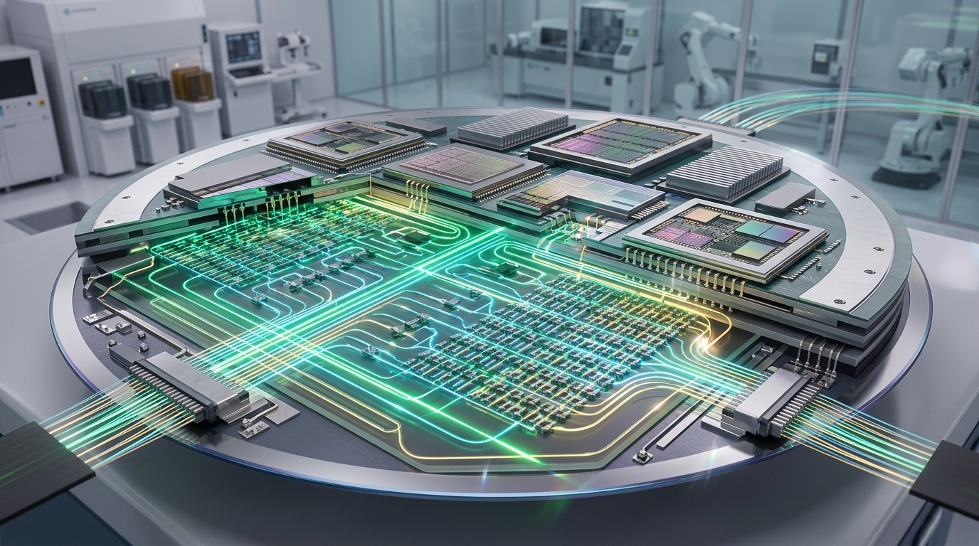
- Lightmatter Passage: The world’s first wafer-scale programmable 3D silicon photonics interposer platform. Rather than routing data through resistive copper wires, Passage integrates microscopic optical waveguides directly into a full three-hundred-millimeter silicon wafer, connecting co-packaged compute chiplets, memory, and switches with tens to hundreds of terabits per second of optical bandwidth.
- Lightmatter Envise: An electro-optic computing architecture that harnesses Mach-Zehnder Interferometers (MZIs) to execute deep learning matrix multiplications at the speed of light using photon interference, operating with near-zero heat dissipation.
By partnering with GlobalFoundries to manufacture these photonic platforms on the commercial GF Fotonix silicon photonics CMOS process, Lightmatter transitioned optical computing from academic physics experiments into mass-production datacenter hardware.
+----------------------------------------------------------------------------------------------------+
| LIGHTMATTER PHOTONIC SUPERCOMPUTING PLATFORM ARCHITECTURE                                          |
+----------------------------------------------------------------------------------------------------+
|                                                                                                    |
|  +----------------------------------------------------------------------------------------------+  |
|  | COMPUTE & MEMORY CHIPLETS (GPUs, Custom ASICs, TPUs, HBM3e/HBM4 Stacks)                       |  |
|  | - Heterogeneous processing dies attached via 3D micro-bumps directly onto the optical wafer  |  |
|  +----------------------------------------------------------------------------------------------+  |
|                                                ||||||||||||||||||||||||||||||||||                  |
|  ======== 3D WAFER-LEVEL HYBRID BONDING: High-Density Micro-Bumps (Direct E-to-O Interface) ======  |
|                                                ||||||||||||||||||||||||||||||||||                  |
|  +----------------------------------------------------------------------------------------------+  |
|  | LIGHTMATTER PASSAGE: WAFER-SCALE 3D SILICON PHOTONICS INTERPOSER (300mm Monolithic Substrate)  |  |
|  | - Microscopic Low-Loss Optical Waveguides routing coherent laser light across entire wafer   |  |
|  | - 114 Tbps to 128 Tbps Aggregate Cross-Sectional Optical Bandwidth                           |  |
|  | - Integrated Electro-Optic Modulators and Sub-Nanosecond Photodetectors                       |  |
|  | - Dynamically Reconfigurable Optical Circuit Switching Matrix (Zero Packet Queuing Buffers)  |  |
|  +----------------------------------------------------------------------------------------------+  |
|                                                ^                                                   |
|                                                | (Direct Low-Loss Optical Ribbon Fibers)           |
|                                                v                                                   |
|  +----------------------------------------------------------------------------------------------+  |
|  | MULTI-RACK SCALE-UP DOMAIN: Seamless Rack-to-Rack Optical Waveguide Trunks (UALink / PCIe)   |  |
|  +----------------------------------------------------------------------------------------------+  |
|                                                                                                    |
+----------------------------------------------------------------------------------------------------+ 1. The Physics of Silicon Photonics: Light as the Ultimate Interconnect
Photons possess physical properties that make them fundamentally superior to electrons for high-speed information transport:
- Zero Resistance and Capacitance: Unlike electrons flowing through copper, photons traveling through silicon dioxide waveguides encounter zero electrical resistance, zero capacitive charging delays, and zero dielectric skin-effect losses.
- Wavelength Division Multiplexing (WDM): Multiple distinct data streams encoded onto different wavelengths (colors) of laser light can travel simultaneously through a single optical waveguide without interfering with one another. A single physical optical channel can carry thirty-two or sixty-four independent high-speed data lanes concurrently, multiplying spatial bandwidth density by orders of magnitude.
- Energy-Distance Invariance: The energy required to transmit an optical pulse across a silicon interposer or across an entire server rack is essentially invariant with distance. While copper power dissipation scales quadratically with length, optical transport consumes less than 0.5 picojoules per bit, delivering a 6x reduction in interconnect power compared to copper SerDes.
2. Flattening the Datacenter Network Hierarchy
By turning the entire silicon interposer into an optical routing fabric, Lightmatter Passage fundamentally flattens the datacenter network architecture:
- Traditional clusters require six to seven layers of electronic packet switches to route data between thousands of compute nodes.
- Passage replaces intermediate electrical packet switches with an integrated Optical Circuit Switching matrix. Photons flow directly from source processor to destination processor through optical waveguides without converting back and forth between optical and electrical domains at every hop.
- This flattens the network hierarchy down to two layers, eliminating packet buffering queues and reducing inter-node communication latencies from microseconds down to sub-nanoseconds.
Deep Architectural Analysis of Lightmatter Passage & Envise Subsystems
To understand how Lightmatter delivers unprecedented throughput and energy efficiency, we examine the physical microarchitecture of the Passage M1000 optical interposer, the electro-optic modulation interfaces, the Mach-Zehnder Interferometer compute meshes, and the UALink consortium integration.
+----------------------------------------------------------------------------------------------------+
| DETAILED ARCHITECTURAL BLOCK DIAGRAM: LIGHTMATTER PASSAGE M1000 & ELECTRO-OPTIC CO-PACKAGING       |
+----------------------------------------------------------------------------------------------------+
|                                                                                                    |
|  +-------------------------+  +-------------------------+     +-------------------------+          |
|  | Processor Chiplet A     |  | Processor Chiplet B     |     | High-Bandwidth Memory   |          |
|  | (Custom ASIC / GPU Die) |  | (Custom ASIC / GPU Die) |     | (HBM3e / HBM4 Stack)    |          |
|  +-------------------------+  +-------------------------+     +-------------------------+          |
|               |                            |                               |                       |
|               v                            v                               v                       |
|  +----------------------------------------------------------------------------------------------+  |
|  | ELECTRICAL-TO-OPTICAL (E-O) INTERFACE CELLS (Under-Die Micro-Bump Arrays)                     |  |
|  | - High-Speed Micro-Ring Resonators (MRR) modulating continuous-wave laser light               |  |
|  | - Integrated Germanium Photodetectors converting optical pulses back to sub-volt electrical logic|  |
|  +----------------------------------------------------------------------------------------------+  |
|                                                ^                                                   |
|                                                | (Photonic Waveguides: Sub-0.1 dB/cm Loss)         |
|                                                v                                                   |
|  +----------------------------------------------------------------------------------------------+  |
|  | PASSAGE MONOLITHIC PHOTONIC INTERPOSER LAYER (Wafer-Scale 300mm Silicon Platform)            |  |
|  | - 114 Tbps Sustained Bi-Directional Optical Routing Capacity                                  |  |
|  | - Programmable Optical Crosspoints: Dynamically steering multi-wavelength light beams        |  |
|  | - External Laser Source (ELS) Optical Power Supply coupling via single-mode fiber arrays     |  |
|  +----------------------------------------------------------------------------------------------+  |
|                                                ^                                                   |
|                                                | (Optical Circuit Switching)                       |
|                                                v                                                   |
|  +----------------------------------------------------------------------------------------------+  |
|  | MACH-ZEHNDER INTERFEROMETER (MZI) COMPUTATIONAL MESH (Envise Optical Core)                  |  |
|  | - 2D Grid of Phase-Shifting Interferometers executing analog linear matrix multiplication    |  |
|  | - Wavelength Division Multiplexing executing multiple tensor dot products in parallel        |  |
|  +----------------------------------------------------------------------------------------------+  |
|                                                                                                    |
+----------------------------------------------------------------------------------------------------+ 1. Passage M1000: The 114 Tbps Wafer-Scale Optical Interconnect
The Passage M1000 represents the pinnacle of 3D silicon photonics integration:
- 300mm Wafer-Scale Substrate: Rather than dicing a processed wafer into microscopic chips, Passage utilizes an entire monolithic 300mm silicon wafer as an active optical interposer.
- Massive Aggregate Bandwidth: The optical interposer features thousands of microscopic single-mode optical waveguides fabricated using the GF Fotonix platform, delivering up to 114 terabits per second (Tbps) of sustained cross-sectional bandwidth across the wafer surface.
- Direct 3D Heterogeneous Co-Packaging: Processors, GPUs, custom AI ASICs, and High-Bandwidth Memory stacks are mounted directly on top of the Passage wafer using ultra-fine micro-bumps. This co-packaged architecture eliminates long PCB copper traces entirely; electrical signals travel less than one millimeter from the transistor logic into the optical modulation cells.
- External Laser Sources (ELS): To isolate heat-sensitive laser diodes from the thermal dissipation of high-wattage compute dies, continuous-wave laser power is supplied by external, field-replaceable laser modules connected via blind-mate optical fiber connectors.
2. High-Speed Optical Modulation and Detection Interfaces
Data translation between the electronic and optical domains occurs at picosecond speeds within localized interface cells embedded under each chiplet footprint:
- Micro-Ring Resonators (MRRs): Electrical voltage signals drive microscopic silicon ring resonators positioned adjacent to optical waveguides. By applying an electrical charge across the ring’s PN-junction, the refractive index of the silicon shifts, modulating the continuous laser beam with zero-latency on-off keying or PAM4 optical pulses.
- Germanium-on-Silicon Photodetectors: At the receiving chiplet, high-responsivity germanium photodetectors absorb incoming light pulses, generating instantaneous photocurrent that is amplified by transimpedance amplifiers back into standard digital logic levels.
- Sub-Nanosecond Time-of-Flight: Because light travels through silicon dioxide at approximately two-thirds the speed of light in a vacuum (~200,000 kilometers per second), a data packet traverses the entire 300mm wafer in less than 1.5 nanoseconds, delivering memory-like access latencies across physically separate chips.
3. Lightmatter Envise: Optical Matrix Multiplication via Mach-Zehnder Interferometry
While Passage provides the optical interconnect fabric, Lightmatter’s Envise architecture executes linear mathematical calculations directly in the optical domain:
- The Mach-Zehnder Interferometer (MZI): An MZI consists of an input optical splitter that divides an incoming coherent laser beam into two separate waveguide arms, followed by an electro-optic phase shifter and a recombiner:
- When an electrical control voltage is applied to the phase shifter, the speed of light through that arm slows down microscopically, shifting the wave’s phase relative to the other arm.
- When the two light beams recombine at the output coupler, they undergo constructive or destructive interference. The intensity of the exiting light is mathematically proportional to the product of the input light amplitude and the programmed phase weight.
- 2D Interferometer Meshes: By cascading hundreds of MZIs into a two-dimensional grid, the optical mesh implements complete Singular Value Decomposition (SVD) matrix multiplication ($Y = U \cdot \Sigma \cdot V^* \cdot X$).
- Speed-of-Light Calculation: Calculations occur passively as the wavefront propagates through the silicon waveguide grid. Once the laser light enters the mesh, the matrix multiplication completes in the time it takes photons to travel across the chip (under 100 picoseconds), consuming zero dynamic capacitive charging power.
- WDM Parallelism: By injecting multiple laser wavelengths simultaneously, the identical physical MZI mesh computes multiple independent tensor dot products at the same time, multiplying arithmetic compute density without increasing silicon area.
+----------------------------------------------------------------------------------------------------+
| THE MACH-ZEHNDER INTERFEROMETER (MZI) OPTICAL COMPUTING CELL                                       |
+----------------------------------------------------------------------------------------------------+
|                                                                                                    |
|                             +--- Upper Arm (Phase Shifter: Δφ) ---+                                |
|                             |    Controlled by Matrix Weight W    |                                |
|                             |                                     |                                |
|  Input Light Vector X ----->|                                     |-----> Output Light Y = W * X   |
|  (Laser Amplitude Encoding) |                                     |       (Constructive/           |
|                             |                                     |        Destructive Interference|
|                             +--- Lower Arm (Reference Phase) -----+                                |
|                                                                                                    |
|  Physics Principle: Multiplication is performed by constructive and destructive interference        |
|  Propagation Latency: <100 picoseconds (Speed of Light through Silicon Waveguides)                 |
|  Dynamic Power Dissipation: 0 Joules during photon traversal                                       |
+----------------------------------------------------------------------------------------------------+ 4. UALink Consortium and Unified Memory Fabrics
In January 2025, Lightmatter joined the Ultra Accelerator Link (UALink) Consortium as a Contributor member:
- Standardized Scale-Up Protocol: UALink defines an open, high-speed accelerator interconnect standard designed to break proprietary lock-in (such as NVIDIA NVLink).
- Photonic UALink Implementation: Lightmatter maps the UALink scale-up protocol directly over Passage optical waveguides. This enables clusters of up to 1,024 heterogeneous accelerators (AMD Instinct GPUs, custom AI ASICs, and CPU host complexes) to share a single, unified memory address space with hardware-level cache coherency across optical links.
Hands-On Idiom Compiler & PyTorch Optical Integration Guide
Developing software for photonic computing must not require artificial intelligence engineers to learn optical physics. Lightmatter developed the Idiom Compiler & SDK, which seamlessly translates standard PyTorch, TensorFlow, and ONNX computational graphs into optical phase configurations, laser power settings, and host runtime schedules.
+----------------------------------------------------------------------------------------------------+
| LIGHTMATTER IDIOM COMPILER & RUNTIME SOFTWARE STACK                                                |
+----------------------------------------------------------------------------------------------------+
| FRONTEND FRAMEWORK: PyTorch 2.x (torch.compile), ONNX Runtime, Hugging Face Transformers           |
+----------------------------------------------------------------------------------------------------+
                                         |
+----------------------------------------------------------------------------------------------------+
| IDIOM GRAPH COMPILER: Graph Partitioning & Electro-Optic Separation                                |
| - Separates linear GEMM operations (Optical Domain) from non-linear activations (Electrical Domain)|
| - SVD Weight Decomposition: Factors weight matrices into unitary MZI phase configurations          |
+----------------------------------------------------------------------------------------------------+
                                         |
+----------------------------------------------------------------------------------------------------+
| PHOTONIC KERNEL COMPILER & CALIBRATION: Phase Voltage Mapping & Thermal Drift Compensation         |
| - Pre-calculates thermal phase shifts and laser wavelength assignments (WDM scheduling)            |
+----------------------------------------------------------------------------------------------------+
                                         |
+----------------------------------------------------------------------------------------------------+
| RUNTIME & DRIVER: UALink / PCIe User-Space Optical Driver & Hardware Transceiver Orchestrator      |
+----------------------------------------------------------------------------------------------------+
                                         |
+----------------------------------------------------------------------------------------------------+
| PHYSICAL HARDWARE: Lightmatter Passage M1000 Optical Interposer & Envise Photonic Compute Core     |
+----------------------------------------------------------------------------------------------------+ 1. Serving Foundation Models with PyTorch and Idiom Optical Backend
Because Lightmatter’s Idiom compiler integrates directly into PyTorch via torch.compile, developers can compile standard transformer architectures for execution across optical compute meshes and Passage interconnects:
# ============================================================================
# File: serve_photonic_model.py
# Description: Production LLM Inference on Lightmatter Passage / Envise Hardware
# Framework: PyTorch 2.x / Lightmatter Idiom SDK / UALink Photonic Runtime
# ============================================================================

import os
import torch
import torch.nn as nn
from typing import Optional

# Configure Lightmatter Idiom Photonic Runtime Flags
os.environ["IDIOM_TARGET_HARDWARE"] = "passage_m1000"
os.environ["IDIOM_OPTICAL_PRECISION"] = "fp16_equivalent"
os.environ["IDIOM_WDM_CHANNELS"] = "16"

class PhotonicTransformerLinear(nn.Module):
    # Linear projection layer compiled for execution on Lightmatter's
    # Mach-Zehnder Interferometer (MZI) optical mesh.
    def __init__(self, in_features: int, out_features: int):
        super().__init__()
        self.in_features = in_features
        self.out_features = out_features
        self.weight = nn.Parameter(torch.randn(out_features, in_features) * 0.02)
        self.bias = nn.Parameter(torch.zeros(out_features))

    def forward(self, x: torch.Tensor) -> torch.Tensor:
        # Step 1: Input tensor is digitized and converted into optical laser amplitudes
        # Step 2: Linear GEMM executes passively across MZI mesh at the speed of light
        # Step 3: Germanium photodetectors digitize output back to electrical registers
        return torch.matmul(x, self.weight.t()) + self.bias

class PhotonicAttentionBlock(nn.Module):
    # Multi-Head Attention block utilizing Passage optical interconnects
    # for zero-latency inter-chip KV-cache routing and optical GEMM execution.
    def __init__(self, hidden_dim: int, num_heads: int):
        super().__init__()
        self.hidden_dim = hidden_dim
        self.num_heads = num_heads
        self.head_dim = hidden_dim // num_heads

        # Projections mapped directly to Photonic MZI mesh
        self.q_proj = PhotonicTransformerLinear(hidden_dim, hidden_dim)
        self.k_proj = PhotonicTransformerLinear(hidden_dim, hidden_dim)
        self.v_proj = PhotonicTransformerLinear(hidden_dim, hidden_dim)
        self.out_proj = PhotonicTransformerLinear(hidden_dim, hidden_dim)
        self.norm = nn.LayerNorm(hidden_dim)

    def forward(self, x: torch.Tensor, mask: Optional[torch.Tensor] = None) -> torch.Tensor:
        residual = x
        normed = self.norm(x)
        b, s, _ = normed.shape

        # Execute Query, Key, Value Projections through optical waveguides
        q = self.q_proj(normed).view(b, s, self.num_heads, self.head_dim).transpose(1, 2)
        k = self.k_proj(normed).view(b, s, self.num_heads, self.head_dim).transpose(1, 2)
        v = self.v_proj(normed).view(b, s, self.num_heads, self.head_dim).transpose(1, 2)

        # Scaled Dot-Product Attention
        scores = torch.matmul(q, k.transpose(-2, -1)) / (self.head_dim ** 0.5)
        if mask is not None:
            scores = scores + mask

        attn = torch.softmax(scores, dim=-1)
        context = torch.matmul(attn, v)
        context = context.transpose(1, 2).contiguous().view(b, s, self.hidden_dim)

        output = self.out_proj(context)
        return output + residual

def compile_for_lightmatter_passage(model: nn.Module) -> nn.Module:
    print("Initiating Idiom Photonic Graph Compilation...")
    # Compile model using PyTorch 2.x Idiom backend
    # Idiom decomposes weight matrices into Singular Value Decomposition (SVD)
    # phase configurations for Mach-Zehnder Interferometer meshes.
    compiled = torch.compile(
        model,
        backend="inductor",
        options={
            "inductor.hardware_target": "lightmatter_photonic",
            "photonic.enable_wdm_parallelism": True,
            "photonic.mzi_mesh_optimization": True,
            "photonic.passage_interposer_routing": "direct_waveguide"
        }
    )
    return compiled

def execute_photonic_inference_session():
    print("Initializing Lightmatter Passage M1000 Photonic Cluster...")

    # Model Configuration
    BATCH_SIZE = 8
    SEQ_LEN = 1024
    HIDDEN_DIM = 2048
    NUM_HEADS = 16

    # Instantiate Photonic Model
    attention_layer = PhotonicAttentionBlock(hidden_dim=HIDDEN_DIM, num_heads=NUM_HEADS)
    attention_layer.eval()

    # Apply Photonic Compilation
    optimized_layer = compile_for_lightmatter_passage(attention_layer)

    # Generate Synthetic Input Tensors
    dummy_tokens = torch.randn(BATCH_SIZE, SEQ_LEN, HIDDEN_DIM, dtype=torch.float32)

    print("Executing Inference Across Photonic Silicon Interposer...")
    with torch.no_grad():
        output = optimized_layer(dummy_tokens)
        print(f"Photonic Execution Successful. Output Dimensions: {output.shape}")

    print("Lightmatter Passage Session Completed.")

if __name__ == "__main__":
execute_photonic_inference_session() 2. Monitoring Photonic Laser Power and Thermal Tuning
Because silicon’s refractive index is sensitive to ambient thermal fluctuations, Lightmatter incorporates active closed-loop thermal phase tuning:
# ============================================================================
# Script: monitor_passage_telemetry.sh
# Description: Monitor Lightmatter Passage optical link health and laser status
# ============================================================================

# Query Lightmatter System Management CLI (lmsmi)
echo "Querying Lightmatter Passage M1000 System Status..."
lmsmi --query-optical-links

# Expected Output Metrics:
# 1. Optical Link Status: Active (114 Tbps Cross-Sectional Bandwidth)
# 2. External Laser Source (ELS) Optical Power: 18.5 dBm per wavelength
# 3. Waveguide Insertion Loss: <0.08 dB/cm (Nominal)
# 4. MZI Phase Tuner Drift Compensation: Locked (Sub-0.01 Radian Stability)
# 5. Interposer Temperature: 42.5°C (Maintained by Liquid Cold Plate) Architectural Comparison: Lightmatter Passage vs. NVIDIA NVLink 4 vs. Optical Transceivers
To understand how Lightmatter Passage transforms datacenter connectivity, we compare it head-to-head against traditional electrical GPU interconnects and pluggable optical transceivers:
+----------------------------------------------------------------------------------------------------+
| HARDWARE SPECIFICATIONS COMPARISON: SCALE-UP INTERCONNECT TECHNOLOGIES                             |
+----------------------------------------------------------------------------------------------------+
| Interconnect Metric           | NVIDIA NVLink 4 (H100) | Pluggable Optical (800G)  | Lightmatter Passage    |
+-------------------------------+------------------------+---------------------------+-----------------------+
| Physical Transmission Medium  | Copper PCB / Direct-Att| Multi-Mode Fiber Cables   | Silicon Waveguides    |
| Interconnect Level            | Intra-Chassis (Board)  | Inter-Chassis (Rack-Rack) | Wafer-Scale Interposer|
| Aggregate Module Bandwidth    | 900 GB/s per GPU       | 100 GB/s (800 Gbps)       | 114,000 GB/s (114 Tbps)|
| Energy Consumption (pJ/bit)   | 8.0 - 15.0 pJ/bit      | 15.0 - 25.0 pJ/bit        | < 0.5 pJ/bit          |
| Link Power Dissipation        | ~120W per GPU SerDes   | ~15W per transceiver      | ~50W per scale-up node|
| Transmission Latency          | ~25 - 50 nanoseconds   | ~100 - 500 nanoseconds    | < 1.5 nanoseconds     |
| Switching Hierarchy Depth     | 2 - 3 Layers (NVSwitch)| 5 - 7 Layers (Fat-Tree)   | Flattened (2 Layers)  |
| Reticle Boundary Limit        | Bound to ~3.3x Reticle | External Cable Length     | Full 300mm Wafer Size |
| Co-Packaged Integration       | Passive Silicon Interp | Front-Panel Pluggable     | Active 3D Optical Sub |
| Consortium Standard Support   | Proprietary (NVIDIA)   | IEEE 802.3 Ethernet       | UALink / CXL / PCIe   |
+----------------------------------------------------------------------------------------------------+ 1. Key Architectural Differentiators
Evaluating the core physics and operational economics reveals why optical interposers supersede copper backplanes:
2. Thirty-Fold Reduction in Transport Energy (pJ/bit)
- Breaking the Thermal Bottleneck: While electrical SerDes and pluggable transceivers consume between 10 and 25 picojoules per bit to drive signals through copper or optical fibers, Lightmatter Passage requires less than 0.5 picojoules per bit. This 30x energy reduction prevents accelerators from throttling under communication-heavy collective operations.
3. Hundred-Fold Bandwidth Scaling via Silicon Waveguides
- Escape Density Supremacy: Copper traces on standard circuit boards suffer from severe cross-talk and capacitance when spaced tightly. In contrast, silicon waveguides spaced micrometers apart route multi-wavelength laser beams without electromagnetic interference, unlocking 114 terabits per second of cross-sectional throughput across a single wafer substrate.
4. Direct Optical Circuit Switching vs. Packet Buffer Latency
- Elimination of Queue Tail Jitter: Traditional packet switches require deep SRAM buffers to prevent packet loss during traffic bursts, creating unpredictable millisecond tail latencies. Passage routes data optically through programmable optical crossbars, eliminating packet buffer queues and achieving sub-nanosecond transit times.
Production Deployment & Enterprise Scaling
Deploying silicon photonics supercomputers in enterprise datacenters requires robust optical packaging, external laser thermal management, and reliable manufacturing partnerships.
1. Commercial Manufacturing with GlobalFoundries GF Fotonix
A primary barrier historically facing optical computing was the lack of commercial manufacturing ecosystems. Lightmatter overcame this by partnering with GlobalFoundries:
- Monolithic Photonic-Electronic CMOS: The Passage platform is manufactured on GlobalFoundries’ GF Fotonix silicon photonics platform, combining 300mm optical waveguide lithography with advanced CMOS electrical control logic on a single production line.
- Standardized High-Yield Assembly: Co-packaged dies, micro-rings, and laser couplers are assembled using high-precision automated robotic pick-and-place equipment, achieving commercial semiconductor manufacturing yields.
2. External Laser Source (ELS) Safety & Reliability
In production datacenter racks, laser reliability is managed through strict architectural isolation:
- Decoupled Thermals: Laser diodes degrade rapidly if subjected to temperatures exceeding 60°C. By housing continuous-wave lasers in separate External Laser Source (ELS) modules mounted in the cool intake air path of the rack, laser operating temperatures remain strictly regulated.
- Blind-Mate Optical Quick-Disconnects: Should a laser source experience a component fault, datacenter technicians can hot-swap the modular ELS cassette without powering down the compute blades or disconnecting internal silicon interposers.
3. Decision Matrix: When to Adopt Silicon Photonics vs. Traditional Clusters
Enterprise infrastructure architects should apply this decision framework when planning next-generation cluster deployments:
| Workload & Infrastructure Profile | Recommended Technology | Operational Rationale & Economic Impact |
|---|---|---|
| Trillion-Parameter MoE Foundation Training | Lightmatter Passage (UALink) | 114 Tbps optical interposer eliminates network tail latency bottlenecks during all-to-all expert routing. |
| High-Density Rack-Scale Scale-Up Domains | Lightmatter Passage | Connects 1,024+ accelerators into a unified coherent memory pool without multi-tier electrical switches. |
| Power-Constrained Hyperscale Datacenters | Lightmatter Photonic Computing | 6x lower interconnect power allows facilities with fixed megawatt limits to install 3x more compute density. |
| Sub-Millisecond Multi-Modal Agent Serving | Lightmatter Envise / Passage | Optical matrix execution and sub-nanosecond waveguide transport eliminate DRAM decode latency. |
| Legacy Small-Scale AI Clusters (under 64 nodes) | Traditional Copper / InfiniBand | Standard copper interconnects remain cost-effective for modest cluster sizes where the Copper Wall is not yet reached. |
By replacing the resistive physics of copper with the limitless speed and efficiency of coherent light, Lightmatter Passage and the silicon photonics revolution establish the foundational infrastructure required to scale artificial intelligence into the trillion-parameter era.