Innatera T1 Guide: Neuromorphic Spiking Sensor AI Silicon
The Digitization Dilemma: Why Conventional Microcontrollers Choke on Continuous Sensor Streams
The rapid expansion of edge computing and ambient intelligence into battery-operated consumer electronics, medical wearables, industrial condition monitoring, and smart automotive cabins has encountered an unyielding physical and thermodynamic barrier. Real-world physical environments generate continuous analog sensory signals—such as acoustic sound waves captured by MEMS microphones, high-frequency electromagnetic chirps from millimeter-wave (mmWave) radar sensors, multi-axis kinetic vibrations from industrial motor bearings, and bio-potential electrical voltages from electrocardiogram (ECG) and photoplethysmogram (PPG) sensors.
However, the hardware architectures deployed to process these sensory streams remain bound to an inefficient, four-decade-old digital signal processing paradigm:
- The Energy Penalty of Nyquist-Shannon Oversampling: In conventional embedded systems, analog physical phenomena must first be captured, filtered, and digitized through high-speed Analog-to-Digital Converters (ADCs). To preserve high-frequency signal features without aliasing, ADCs must sample at or above the Nyquist rate, generating millions of digital bits per second. The ADC stage itself frequently burns hundreds of microwatts to several milliwatts simply digitizing background noise when no meaningful physical event is occurring.
- The Digital Signal Processing (DSP) Preprocessing Tax: Once digitized, the raw sensor time-series data cannot be fed directly into deep neural networks. A conventional digital microcontroller (such as an ARM Cortex-M4, Cortex-M33, or DSP core) must wake up, run extensive digital signal processing pipelines—such as computing Fast Fourier Transforms (FFT), calculating short-time Fourier transforms (STFT), running discrete cosine transforms (DCT), or extracting mel-frequency cepstral coefficients (MFCC)—and store intermediate spectral matrices in SRAM. Executing millions of clocked multiply-accumulate (MAC) loops to extract features burns between 10 milliwatts and 100 milliwatts of power, draining small coin-cell or lithium-polymer batteries in a matter of days or weeks.
- The Static Clocked Leakage Wall: Digital processors require high-frequency clock oscillators and extensive multi-level memory buses. Even when operating in low-power idle states, digital flip-flops and static RAM cells experience sub-threshold transistor leakage. In always-on sensing applications—where an acoustic sensor must listen continuously for safety alarms, glass breakage, or voice wake words—continuous digital clocking wastes over 95% of total battery capacity monitoring empty, unchanging environments.
- Cloud-Tethering Latency and Privacy Hazards: Because conventional sub-milliwatt microcontrollers lack the arithmetic capacity to execute modern deep neural networks locally, engineering teams often resort to transmitting raw sensor payloads over Bluetooth Low Energy (BLE), Wi-Fi, or cellular IoT modems to cloud servers. Radio transmission consumes massive peak current (often 10mA to 30mA at 3.3V), introduces unpredictable network latency spikes, and compromises personal biometric and environmental privacy.
To realize true ambient intelligence across billions of battery-powered sensors, the industry requires an entirely different silicon computing architecture: a neuromorphic processor capable of processing analog sensor signals directly in the time domain with sub-milliwatt power dissipation.
Introducing Innatera T1: The World’s First Neuromorphic Microcontroller
The Innatera T1 emerges as an uncompromising, bio-inspired architectural solution to the sensor edge crisis. Developed by semiconductor pioneer Innatera Nanosystems—a spin-off from the prestigious Delft University of Technology (TU Delft) in the Netherlands, led by CEO Sumeet Kumar—the T1 is the world’s first commercially available neuromorphic microcontroller and Spiking Neural Processor (SNP) designed specifically for sensor edge intelligence.
Rather than forcing continuous analog waveforms through power-hungry Nyquist-rate ADCs and digital DSP feature extraction loops, the Innatera T1 processes sensor signals directly in the time domain using an ultra-low-power Analog-Mixed-Signal Spiking Neural Network (Pulsed Neural Network) core. The T1 models the temporal dynamics of biological sensory perception: analog spiking neurons continuously integrate sensory signals as physical electrical charges on microscopic capacitor circuits, firing discrete temporal voltage spikes only when salient sensory patterns occur.
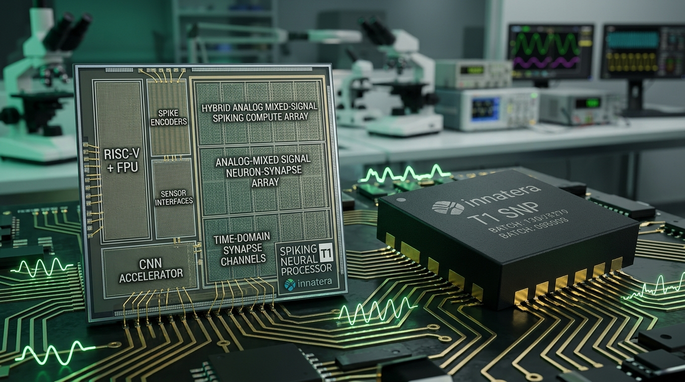
Fabricated on a cost-effective standard TSMC digital CMOS process with mixed-signal extensions, the Innatera T1 integrates an entire heterogeneous edge compute platform onto a single monolithic die:
- Analog-Mixed-Signal Spiking Neural Processor (SNP): Features a massively parallel array of analog spiking neurons and synapses that execute temporal neural inference with near-zero latency, consuming between 50 microwatts ($\mu\text{W}$) and 500 microwatts ($\mu\text{W}$) of typical power—delivering over 100x lower energy consumption than traditional digital microcontrollers.
- Dedicated Digital 2D CNN Hardware Accelerator: A specialized, low-power digital convolutional engine that operates in tandem with the analog spiking core, handling structured 2D spatial feature maps when processing complex multi-dimensional visual or radar range-Doppler matrices.
- Energy-Optimized 32-bit RISC-V Application CPU: An integrated open-standard RISC-V processor core with single-cycle multiply-accumulate and floating-point support, responsible for system initialization, sensor interface control, communication protocol handling, and application decision logic.
- PyTorch-Native Talamo™ Software Development Kit: A comprehensive, production-grade software compiler and development environment that allows machine learning engineers to design, train, quantize, and compile spiking neural networks directly from standard PyTorch and TensorFlow workflows, abstracting away the underlying analog circuit complexities.
Enterprises deploying distributed industrial sensor fleets, predictive maintenance monitors, and remote ambient intelligence nodes can integrate Innatera T1 edge clusters with real-time data ingestion infrastructure to stream validated anomaly events, operational telemetry, and sensory metadata directly into cloud databases. By eliminating power-hungry DSP pre-filtering and computing natively on physical time-domain spikes, the Innatera T1 unlocks continuous, multi-year artificial intelligence on compact coin-cell batteries.
Architectural Deep Dive: Spiking Neural Processor (SNP), Analog Core, and Heterogeneous Silicon
Understanding the revolutionary power-performance profile of the Innatera T1 requires an in-depth examination of its microarchitecture across four interconnected subsystems: the Analog-Mixed-Signal Spiking Compute Array, the heterogeneous RISC-V control complex, the Time-Domain Spike Encoder and Direct Sensor Interfaces, and the mathematical principles governing continuous-time analog neural dynamics.
System Topology of the Innatera T1 Neuromorphic SoC
The physical architecture of the Innatera T1 is structured as a tightly coupled, heterogeneous System-on-Chip (SoC) designed to minimize data movement and eliminate inter-chip communication overhead:
+-----------------------------------------------------------------------+
|                       Innatera T1 Neuromorphic SoC                    |
+-----------------------------------------------------------------------+
|  +------------------------+  +-------------------------------------+  |
|  | Multi-Channel Direct   |  | Energy-Efficient 32-Bit RISC-V CPU  |  |
|  | Sensor Interfaces      |  | - 32-Bit IMC Core with Hardware MAC |  |
|  | - I2S, PDM (Audio)     |  | - 128KB Low-Leakage System SRAM     |  |
|  | - SPI, I2C, UART       |  | - Power Management & Clock Gating   |  |
|  | - Analog Front-End ADC |  | - Autonomous DMA Controller         |  |
|  +-----------+------------+  +------------------+------------------+  |
|              |                                  |                     |
|  +-----------v----------------------------------v------------------+  |
|  |               Asynchronous Event & Memory Interconnect          |  |
|  +-----------------------------------------------------------------+  |
|        |                  |                  |                  |     |
|  +-----v-----+      +-----v-----+      +-----v-----+      +-----v-----+  |
|  | Time-     |      | Analog    |      | Digital   |      | Hardware  |  |
|  | Domain    |      | Spiking   |      | 2D CNN    |      | Watchdog  |  |
|  | Spike     |----->| Neural    |----->| Co-       |----->| & System  |  |
|  | Encoders  |      | Array     |      | Processor |      | Sequencer |  |
|  | (Delta)   |      | (PNN)     |      | (Spatial) |      | Engine    |  |
|  +-----------+      +-----------+      +-----------+      +-----------+  |
+-----------------------------------------------------------------------+ Incoming sensory signals flow from external microphones, radar transceivers, or inertial measurement units (IMUs) through dedicated direct sensor interfaces. If the input is analog, on-chip ultra-low-power signal conditioning stages route the waveform into the Time-Domain Spike Encoders, converting continuous voltages into asynchronous event streams. The event streams are injected directly into the Analog Spiking Neural Array, executing pattern recognition entirely in the analog domain before waking the RISC-V CPU only when an actionable classification is confirmed.
The Analog-Mixed-Signal Spiking Neural Array
At the core of the Innatera T1 is the proprietary Spiking Neural Processor (SNP) compute array. Unlike traditional digital accelerators that simulate neuron equations through discrete numerical integration ($V[t] = V[t-1] + \Delta t \dots$), the T1 uses the intrinsic physical physics of sub-threshold CMOS transistors to execute neuromorphic equations directly.
The analog spiking core features:
- Continuous-Time Leaky Integrate-and-Fire (LIF) Neurons: Implemented using ultra-low-leakage analog capacitor and operational transconductance amplifier (OTA) circuits. Synaptic input currents charge an analog membrane capacitor, while an adjustable resistive leak path continuously dissipates charge, naturally modeling temporal decay without requiring digital multiplication or clock cycles.
- Non-Volatile and SRAM-Assisted Synaptic Weight Arrays: Synaptic connection weights ($W_{ij}$) are stored in local, highly compact static memory cells that control programmable transconductance current sources. When an incoming spike arrives, it pulses the transconductance cell, injecting an exact quantum of electrical charge ($Q = I_{syn} \cdot \Delta t$) into the postsynaptic neuron’s membrane capacitor.
- Asynchronous Inter-Neuron Event Routing: Neurons communicate across layers using discrete digital spike pulses transmitted over an unclocked, self-timed asynchronous event bus. Because no clock grid is distributed across the analog array, static dynamic switching power is completely eliminated.
Mathematical Foundations of Analog Time-Domain Neuromorphic Dynamics
The physics of biological neural membranes is governed by continuous differential equations. The Innatera T1 maps these equations directly onto analog physical circuits, described mathematically by the continuous-time Leaky Integrate-and-Fire formulation:
$$C_m \frac{d V_i(t)}{dt} = - g_L (V_i(t) - E_L) + I_{syn,i}(t)$$
where:
- $C_m$ is the physical capacitance of the integrated on-chip analog membrane capacitor (typically tens to hundreds of femtofarads, $\text{fF}$).
- $V_i(t)$ represents the instantaneous analog voltage across the membrane capacitor of neuron $i$.
- $g_L$ represents the programmable sub-threshold leakage conductance, establishing the biological membrane time constant $\tau_m = \frac{C_m}{g_L}$.
- $E_L$ is the resting reversal potential.
- $I_{syn,i}(t)$ represents the aggregate synaptic current injected into neuron $i$ by incoming presynaptic spikes.
The total synaptic current is the linear superposition of exponentially decaying post-synaptic current pulses generated by presynaptic spike arrival times ${t_j^{(k)}}$:
$$I_{syn,i}(t) = \sum_{j \in \mathcal{P}i} W{ij} \sum_{k} \alpha(t - t_j^{(k)}) \cdot \Theta(t - t_j^{(k)})$$
where $W_{ij}$ is the synaptic weight scalar, $\Theta(t)$ is the Heaviside step function, and $\alpha(t) = \frac{t}{\tau_s} \exp\left(-\frac{t}{\tau_s}\right)$ represents the post-synaptic current response curve with synaptic time constant $\tau_s$.
When the analog membrane voltage $V_i(t)$ charges up and crosses a calibrated physical comparator threshold voltage $V_{th}$:
$$V_i(t) \ge V_{th} \implies \text{Fire Spike at time } t^{(m)}, \quad V_i(t) \leftarrow V_{reset}$$
The analog comparator triggers a digital monostable multivibrator that emits a 1-bit spike pulse onto the asynchronous event bus and resets the membrane potential to $V_{reset}$ for a refractory period $t_{ref}$.
Because the integration of incoming signals and the exponential decay are performed by the natural movement of physical electrons across analog capacitors and transistors, zero mathematical calculations are executed by an ALU. The energy consumed per synaptic operation ($E_{syn}$) drops to under 1 to 5 picojoules (pJ)—more than two orders of magnitude below digital systolic arrays.
Time-Domain Spike Encoders and Direct Sensor Interfacing
To process raw sensor signals without digital DSP preprocessing, the Innatera T1 incorporates proprietary Time-Domain Spike Encoders. For acoustic audio and vibrational acceleration streams, the T1 supports both level-crossing (Delta) encoding and Temporal Contrast encoding:
- Asynchronous Delta Modulators: Continuously track incoming analog sensor voltages. When the signal increases by a programmable step voltage $+\Delta V$, an “ON” spike event is emitted; when the signal decreases by $-\Delta V$, an “OFF” spike event is emitted. The temporal density and inter-spike intervals of the events preserve both the amplitude and spectral frequency content of the physical waveform without requiring an FFT.
- Direct Digital Audio Ingestion (PDM / I2S): For digital MEMS microphones, the T1 ingests 1-bit Pulse-Density Modulated (PDM) bitstreams directly into a hardware decimation-spike converter, transforming high-frequency bit patterns into sparse spiking events in real time.
- Millimeter-Wave (mmWave) Radar Range-Doppler Processing: For radar sensing, the T1 couples its analog spiking array with the digital 2D CNN co-processor. The analog spiking core monitors continuous raw radar intermediate-frequency (IF) chirps to detect human presence or micro-motion, activating the 2D CNN only when complex gesture or trajectory classification is required.
Practical Implementation: Compiling Spiking Sensor Pipelines with the Talamo SDK
Developing, training, and deploying neural network models onto the Innatera T1 is managed through the Talamo™ SDK. Talamo is a comprehensive, Python-native framework built on top of PyTorch that allows developers to design spiking neural networks, train them using surrogate gradient backpropagation, perform hardware-aware calibration, and compile native binaries for the T1 SoC.
End-to-End Spiking Audio Keyword Spotting Pipeline
The following Python script illustrates how to use the Talamo SDK to define a Spiking Neural Network for audio keyword spotting (e.g., detecting wake words or acoustic safety alarms), train it with surrogate gradients, calibrate it for the analog spiking array, and export a hardware executable:
#!/usr/bin/env python3
# Innatera T1 Audio Keyword Spotting and SNN Compilation Script
# Trains a Spiking Neural Network in PyTorch and compiles for the T1 Neuromorphic SoC.

import os
import sys
import torch
import torch.nn as nn
import talamo
import talamo.nn as tnn
import talamo.compiler as tc

class SpikingKeywordSpotter(talamo.Module):
    """
    Bio-inspired Spiking Neural Network architecture for audio wake-word detection.
    Operates on streaming time-domain spikes with sub-500uW power dissipation.
    """
    def __init__(self, num_input_channels=32, num_classes=4):
        super().__init__()
        # Layer 1: Time-domain spatial-temporal spiking convolution
        self.conv1 = tnn.SpikingConv1d(
            in_channels=num_input_channels,
            out_channels=64,
            kernel_size=5,
            stride=1,
            padding=2,
            neuron_model=tnn.LIFNeuron(tau_mem=15e-3, v_th=1.0)
        )

        # Layer 2: Recurrent Spiking Synaptic Pool for long-term temporal context
        self.dense_snn = tnn.SpikingDense(
            in_features=64,
            out_features=128,
            neuron_model=tnn.LIFNeuron(tau_mem=25e-3, v_th=1.0)
        )

        # Layer 3: Output Classification Readout Layer
        self.readout = tnn.NonSpikingDense(
            in_features=128,
            out_features=num_classes
        )

    def forward(self, spike_stream):
        # spike_stream shape: [batch_size, time_steps, channels]
        x, _ = self.conv1(spike_stream)
        x, _ = self.dense_snn(x)
        # Integrate spikes over the time window to derive classification logits
        logits = self.readout(x.mean(dim=1))
        return logits

def compile_and_export_t1_binary(model_weights_path: str, output_bin_path: str):
    print(f"[Talamo] Initializing Innatera T1 compilation session...")
    device_target = talamo.HardwareTarget(soc_type="T1-SNP-QFN")

    # 1. Instantiate and Load Trained PyTorch SNN Model
    model = SpikingKeywordSpotter(num_input_channels=32, num_classes=4)
    model.load_state_dict(torch.load(model_weights_path, map_location="cpu"))
    model.eval()
    print("[Talamo] PyTorch SNN model loaded successfully.")

    # 2. Hardware-Aware Calibration and Analog Variation Profiling
    print("[Talamo] Running analog circuit variation calibration and threshold tuning...")
    calibrator = talamo.HardwareCalibrator(target=device_target)
    calibrated_model = calibrator.calibrate(
        model,
        target_operating_temp_c=35.0,
        leakage_trim_mode=talamo.LeakageTrim.OPTIMAL_SUB_MILLIWATT
    )

    # 3. Compile Graph to Innatera Spiking Neural Processor Micro-Code
    compiler_options = tc.CompilerConfig(
        optimization_level=tc.OptLevel.POWER_FIRST,
        enable_direct_pdm_microphone_ingest=True,
        riscv_wake_threshold_confidence=0.85, # Only wake RISC-V CPU on high confidence
        power_budget_uw=350.0 # Strict 350 microwatt power budget
    )

    print("[Talamo] Mapping analog synapses and programming on-chip LIF parameters...")
    t1_executable = tc.build(calibrated_model, compiler_options)

    # 4. Export Binary Artifact for Flashing
    t1_executable.export_binary(output_bin_path)
    print(f"[Talamo] Compilation complete! Output saved to: {output_bin_path}")
    print(f"[Talamo] Estimated Typical Power: {t1_executable.metrics.estimated_power_uw:.1f} uW | "
          f"Inference Latency: {t1_executable.metrics.decision_latency_ms:.2f} ms")

if __name__ == "__main__":
    # Create dummy checkpoint for demonstration
    dummy_model = SpikingKeywordSpotter()
    torch.save(dummy_model.state_dict(), "kws_snn_weights.pth")

compile_and_export_t1_binary("kws_snn_weights.pth", "keyword_spotter_t1.bin") Embedded C Firmware for the T1 RISC-V Application Core
Once compiled, the binary executable runs autonomously on the Innatera T1 hardware. The integrated RISC-V processor remains in deep sleep, waking only when the analog spiking core detects a verified target event. The following C firmware demonstrates the event-driven interrupt lifecycle on the T1 microcontroller:
/**
 * Innatera T1 Embedded RISC-V Firmware
 * Manages low-power sensor ingestion, SNP hardware interrupts, and system dispatch.
 */

#include <stdio.h>
#include <stdint.h>
#include <stdbool.h>
#include "t1_hal.h"
#include "t1_snp_driver.h"
#include "t1_power_mgmt.h"

// Callback executed by hardware interrupt when SNP detects an acoustic keyword
static volatile bool g_keyword_detected = false;
static volatile uint8_t g_detected_class_id = 0;
static volatile float g_detection_confidence = 0.0f;

void SNP_Detection_IRQHandler(void) {
    // Clear hardware interrupt flag
    t1_snp_clear_interrupt();

    // Read inference result registers directly from the analog readout stage
    t1_snp_get_classification_result(&g_detected_class_id, &g_detection_confidence);
    g_keyword_detected = true;
}

int main(void) {
    // 1. Initialize System Clocks and Low-Power Domain
    t1_system_init();
    t1_power_configure_domain(T1_PWR_ANALOG_CORE, T1_PWR_STATE_ON);
    t1_power_configure_domain(T1_PWR_CNN_ACCELERATOR, T1_PWR_STATE_OFF); // Power gate CNN until needed

    printf("[System] Innatera T1 Neuromorphic MCU Booted.\n");

    // 2. Load Compiled SNN Neural Configuration into Analog SNP Array
    if (t1_snp_load_network("keyword_spotter_t1.bin") != T1_OK) {
        printf("[Error] Failed to initialize SNP neural network.\n");
        return -1;
    }

    // 3. Configure Direct Digital MEMS Microphone Interface (PDM)
    t1_pdm_config_t pdm_cfg = {
        .sample_rate_hz = 16000,
        .clock_freq_hz = 1024000,
        .gain_db = 12,
        .direct_route_to_snp = true // Route raw audio pulses directly to analog spike encoder
    };
    t1_pdm_init(&pdm_cfg);

    // 4. Register Hardware Interrupt and Arm Spiking Core
    t1_snp_register_callback(SNP_Detection_IRQHandler);
    t1_snp_enable_inference();

    printf("[System] Entering Autonomous Sub-Milliwatt Sleep. Monitoring audio...\n");

    // 5. Main Execution Loop: Sleep CPU until Neuromorphic Event
    while (1) {
        // Put the RISC-V application CPU into low-leakage WFI (Wait-For-Interrupt) sleep
        // The analog spiking array continues monitoring at <350 microwatts
        t1_enter_low_power_sleep();

        if (g_keyword_detected) {
            printf("[Alert] Keyword Event Detected in Hardware! Class: %u (Confidence: %.2f)\n",
                   g_detected_class_id, g_detection_confidence);

            // Execute application action (e.g., wake host processor, signal system)
            t1_gpio_set_pin(T1_GPIO_PIN_WAKE_HOST, HIGH);
            t1_delay_ms(10);
            t1_gpio_set_pin(T1_GPIO_PIN_WAKE_HOST, LOW);

            // Reset detection state and return to deep sleep
            g_keyword_detected = false;
        }
    }

    return 0;
} Teams developing automated sensor intelligence networks, distributed environmental loggers, or autonomous field inspection fleets can integrate Innatera T1 edge nodes with automated data harvesting agents to aggregate localized anomaly telemetry, cross-reference environmental logs against remote databases, and synchronize firmware updates. For an architectural analysis of how neuromorphic microcontrollers interface with enterprise backbones, visit our AI engineering knowledge hub.
Architectural Comparison: Innatera T1 vs. Competing Edge Sensor AI Silicon
To evaluate the operational suitability of the Innatera T1 within battery-powered wearables, industrial Internet of Things (IoT) sensors, and smart infrastructure deployments, hardware architects must evaluate competing edge silicon options across power budgets, processing paradigms, sensor interface latency, and energy per inference. The table below benchmarks the Innatera T1 against prominent edge sensor processors: the ARM Cortex-M4 with CMSIS-NN, Syntiant NDP120, Texas Instruments MSP430, and Google Coral Edge TPU.
| Architectural Feature | Innatera T1 | Syntiant NDP120 | ARM Cortex-M4 (CMSIS-NN) | TI MSP430 (Ultra-Low MCU) | Google Coral Edge TPU |
|---|---|---|---|---|---|
| Silicon Architecture | Analog-Mixed-Signal SNP + RISC-V | Syntiant Core 2 + HiFi 3 DSP | Digital RISC MCU + DSP Ext. | 16-Bit Low-Power RISC MCU | 2D Systolic Matrix Array |
| Computing Paradigm | Continuous-Time Spiking (PNN/SNN) | Digital Neural In-Memory (NDP) | Synchronous Clocked Von Neumann | Synchronous Clocked Von Neumann | Synchronous Clocked Matrix |
| Active Power Consumption | 50 $\mu$W - 500 $\mu$W (Sub-milliwatt) | 1 mW - 5 mW | 15 mW - 45 mW | 1.5 mW - 4 mW (No AI) | 2,000 mW (2.0W) |
| Typical Battery Longevity | Years on a single CR2032 coin cell | Months on small battery pack | Weeks on AA battery pack | Years (Basic sensing only) | Hours on heavy battery pack |
| Sensor Signal Processing | Direct Raw Signal Ingest (No FFT) | On-Chip Audio Filterbank | Software FFT / MFCC loops | External Analog Front-End | Host CPU Preprocessing Req. |
| Inference Response Latency | < 1 - 5 Milliseconds | < 10 - 20 Milliseconds | 50 - 150 Milliseconds | > 500 ms (CPU bound) | 5 - 15 Milliseconds |
| Energy per Sensory Inference | < 10 Microjoules ($\mu$J) | ~50 - 100 Microjoules | 1,000 - 3,000 Microjoules | Infeasible for deep neural net | > 10,000 Microjoules |
| Integrated Application CPU | 32-Bit RISC-V Core | Cadence HiFi 3 DSP Core | Integrated Cortex-M4 Core | 16-Bit MSP430 Core | None (Requires Host CPU) |
| Physical Semiconductor Node | TSMC Digital CMOS (Mixed-Signal) | 40nm Standard CMOS | 40nm / 65nm Standard CMOS | 90nm / 130nm FRAM | TSMC 28nm Planar |
| Form Factor and Packaging | Compact QFN / WLCSP Package | 3.1 x 2.5 mm WLCSP | QFP / QFN Package | VQFN Package | M.2 / PCIe / USB Module |
Analysis of Architectural Trade-offs
A detailed examination of this matrix reveals critical design trade-offs governing edge sensor deployment:
- Sub-Milliwatt Operating Envelope vs. Embedded GPUs and TPUs: While accelerators like the Google Coral Edge TPU deliver high peak compute density (4 TOPS), their 2-watt power draw makes continuous battery-powered operation physically impossible. A standard CR2032 coin cell (capacity $\approx 220\text{ mAh}$ at 3V, or $\approx 660\text{ mWh}$) would be drained by a Coral TPU in approximately 20 minutes. In contrast, the Innatera T1 operates continuously at 150 microwatts, allowing uninterrupted neural inference for over six months to several years on a single coin cell.
- Elimination of Digital DSP Feature Extraction: On conventional ARM Cortex-M microcontrollers, computing audio mel-spectrograms or radar range-Doppler maps in software burns over 80% of total inference energy. The Innatera T1 completely bypasses the digital DSP stage: its analog spike encoders directly convert raw continuous signals into temporal event patterns, saving tens of milliwatts of system power.
- Dedicated Heterogeneous Architecture vs. Inflexible Microcontrollers: Pure microcontrollers (such as the TI MSP430 or ARM Cortex-M0+) consume very low static power, but their lack of dedicated tensor acceleration makes executing complex deep learning models impossible. By combining a physical analog spiking core with an application-class RISC-V CPU on the same die, the Innatera T1 delivers high-level programmability alongside neuromorphic energy efficiency.
Production Engineering: Hardware Integration, Sensor Interfacing, and Telemetry Monitoring
Transitioning the Innatera T1 from proof-of-concept prototyping into multi-year commercial deployments—such as smart earbuds, industrial asset trackers, and environmental monitoring grids—requires rigorous attention to electrical noise decoupling, analog layout routing, and automated operational telemetry.
Physical Installation, Printed Circuit Board (PCB) Layout, and Mixed-Signal Isolation
Because the T1 integrates sensitive analog spiking neuron circuits on the same silicon substrate as high-speed digital I/O lines and an operating RISC-V core, hardware layout engineers should observe the following guidelines:
- Split Analog and Digital Power Ground Planes: The PCB design must maintain separated analog ($V_{DDA}$, $V_{SSA}$) and digital ($V_{DDD}$, $V_{SSD}$) ground planes, joined exclusively at a single star-point directly beneath the T1 chip package. This prevents digital switching current transients from coupling into sensitive analog membrane capacitor nodes.
- Low-ESR Decoupling Capacitors: Place high-frequency ceramic decoupling capacitors ($10,\text{nF}$ and $1,\mu\text{F}$, X7R dielectric) within 2 millimeters of the analog power supply pins to suppress switching ripple from external DC-DC switching regulators.
- Direct Differential Sensor Trace Routing: Route analog input traces from MEMS microphones or radar receivers as tightly coupled differential pairs, shielded on adjacent PCB layers by solid ground planes to prevent electromagnetic interference (EMI) from nearby wireless radios (such as Bluetooth, Wi-Fi, or LoRa transceivers).
Production Telemetry and Neuromorphic Health Daemon
In mission-critical industrial deployments, an edge system daemon must monitor the operational health of deployed Innatera T1 microcontrollers, tracking ambient temperature, supply rail voltages, analog baseline drift, and event spike rates. The following Python daemon demonstrates an automated monitoring agent that interfaces with the T1 hardware management API:
#!/usr/bin/env python3
# Innatera T1 Fleet Health and Operational Telemetry Daemon
# Monitors analog core stability, spike event rates, and battery supply voltage.

import time
import logging
import json
import sys
from typing import Dict, Any

# Mock or production import of Innatera Hardware Management Library (IHML)
try:
    import ihml
except ImportError:
    # Simulated IHML interface for testing environments
    class MockIHML:
        class Device:
            def __init__(self, idx): self.idx = idx
            def get_junction_temperature_c(self): return 28.5
            def get_power_consumption_uw(self): return 285.4
            def get_supply_voltage_v(self): return 3.02
            def get_spikes_per_second(self): return 14200
            def get_analog_leakage_drift_pct(self): return 0.4
            def get_riscv_uptime_seconds(self): return 86400
            def recalibrate_analog_baselines(self): pass
            def enter_emergency_standby(self): pass

        @staticmethod
        def init(): pass
        @staticmethod
        def device_count(): return 1
        @staticmethod
        def get_device(idx): return MockIHML.Device(idx)
    ihml = MockIHML

logging.basicConfig(
    level=logging.INFO,
    format='%(asctime)s [%(levelname)s] [T1-MONITOR] %(message)s',
    handlers=[logging.StreamHandler(sys.stdout)]
)

class InnateraHealthMonitor:
    def __init__(self, poll_interval_sec: float = 5.0, min_battery_volts: float = 2.2):
        self.interval = poll_interval_sec
        self.min_battery_volts = min_battery_volts
        ihml.init()
        self.num_devices = ihml.device_count()
        self.devices = [ihml.get_device(i) for i in range(self.num_devices)]
        logging.info(f"Initialized Innatera Monitor for {self.num_devices} detected T1 Neuromorphic MCU(s).")

    def collect_telemetry(self, dev) -> Dict[str, Any]:
        """Polls real-time analog and digital sensor telemetry from the T1 processor."""
        temp = dev.get_junction_temperature_c()
        power_uw = dev.get_power_consumption_uw()
        v_bat = dev.get_supply_voltage_v()
        spike_rate = dev.get_spikes_per_second()
        drift_pct = dev.get_analog_leakage_drift_pct()
        uptime = dev.get_riscv_uptime_seconds()

        return {
            "device_id": dev.idx,
            "junction_temp_c": temp,
            "power_microwatts": power_uw,
            "battery_volts": v_bat,
            "spikes_per_second": spike_rate,
            "analog_drift_pct": drift_pct,
            "uptime_seconds": uptime
        }

    def verify_safety_guards(self, dev, telemetry: Dict[str, Any]):
        """Evaluates battery voltage and analog drift limits."""
        v_bat = telemetry["battery_volts"]
        drift = telemetry["analog_drift_pct"]
        dev_id = telemetry["device_id"]

        # 1. Low Battery Threshold Trigger
        if v_bat <= self.min_battery_volts:
            logging.critical(
                f"Device {dev_id} BATTERY CRITICALLY LOW: {v_bat:.2f}V (Threshold: {self.min_battery_volts:.2f}V)! "
                "Switching T1 to ultra-low leakage standby mode."
            )
            dev.enter_emergency_standby()

        # 2. Analog Drift Verification
        if drift > 5.0:
            logging.warning(
                f"Device {dev_id} detected analog leakage drift of {drift:.1f}%. "
                "Triggering automated background calibration."
            )
            dev.recalibrate_analog_baselines()

    def run_monitor_loop(self):
        """Continuous execution loop emitting telemetry status for IoT telemetry backbones."""
        logging.info("Starting production monitoring cycle...")
        try:
            while True:
                for dev in self.devices:
                    telemetry = self.collect_telemetry(dev)
                    self.verify_safety_guards(dev, telemetry)
                    logging.info(f"Telemetry Status: {json.dumps(telemetry)}")
                time.sleep(self.interval)
        except KeyboardInterrupt:
            logging.info("Terminating Innatera Monitor daemon cleanly.")

if __name__ == "__main__":
    monitor = InnateraHealthMonitor(poll_interval_sec=5.0)
    # Perform single initial diagnostic pass
    for dev in monitor.devices:
        sample = monitor.collect_telemetry(dev)
        print("\n=== Initial Innatera T1 Neuromorphic Diagnostic Pass ===")
        for k, v in sample.items():
            print(f"  {k:24s}: {v}")
        print("========================================================\n")
print("Diagnostic passed. Neuromorphic microcontroller ready for continuous service.") Production Readiness Verification Checklist
Prior to mass commercial deployment of Innatera T1 neuromorphic microcontrollers into industrial or consumer hardware products, engineering teams must verify each operational requirement:
- Ambient Temperature Drift Calibration: Execute thermal profiling across the target operating range (-20°C to +70°C) to verify that on-chip temperature-compensation bias circuits maintain stable analog neuron firing thresholds.
- Acoustic and Sensor Noise Floor Tuning: Calibrate the Time-Domain Spike Encoder step voltage thresholds ($\Delta V$) against environmental background noise to prevent false spike generation during quiet periods.
- Battery Discharge and Dropout Profiling: Test system behavior under real-world battery discharge curves down to 2.0V, verifying that the brown-out detection (BOD) circuitry safely suspends operations without corrupting SRAM weight tables.
- End-to-End Decision Accuracy Verification: Run continuous accuracy regression tests on 5,000 real-world acoustic or radar validation samples, confirming that the compiled spiking model achieves within 0.8% accuracy of the floating-point baseline model.
The Innatera T1 establishes a new paradigm for always-on edge artificial intelligence. By breaking free from the clocked von Neumann cycle and computing directly in the analog time domain using spiking neural dynamics, the T1 slashes sensory processing power consumption to sub-milliwatt levels. For embedded systems engineers and product creators building the next generation of intelligent, battery-operated ambient devices, the Innatera T1 transforms long-standing physical limits into sustainable commercial reality.