Graphcore Bow IPU Guide: 3D Wafer-on-Wafer AI Architecture
The SIMD/SIMT Lock-In and the Curse of Dense Execution
In modern enterprise artificial intelligence platforms, autonomous agent clusters, and high-velocity web harvesting infrastructures powered by AI Fetchly, computational workloads are diversifying far beyond uniform dense tensor operations. While dense transformer architectures remain the industry foundation for general language generation, production intelligence systems increasingly depend on fine-grained, non-uniform structural representations. These complex workloads include traversing volatile enterprise knowledge graphs, parsing deeply nested and dynamic document trees through automated web scraping, orchestrating irregular multi-modal event streams with real-time data ingestion, executing probabilistic Monte Carlo Markov Chain simulations, and running sparse mixture-of-experts routing layers.
For more than fifteen years, accelerated computing has been nearly synonymous with graphics processing units. GPUs owe their massive parallel throughput to an architectural lineage rooted in graphics rasterization, built around Single Instruction, Multiple Threads and wide Single Instruction, Multiple Data execution blocks. While SIMT architectures excel when billions of arithmetic operations perform identical multiply-accumulate steps on contiguous matrices, they encounter catastrophic architectural bottlenecks when confronted with modern sparse, irregular, or graph-structured artificial intelligence workloads.
1. The Warp Divergence Penalty on Sparse and Irregular Graphs
In conventional GPU architectures, individual compute units group parallel threads into fixed lock-step execution blocks called warps, typically comprising thirty-two threads. Every thread within a warp must execute the identical machine instruction at every clock cycle. When algorithms process dense matrix multiplications, all thirty-two threads step through uniform memory offsets and compute dot products in perfect synchronization:
- When an algorithm introduces conditional logic, irregular neighbor counts, or dynamic pruning thresholds, individual threads naturally evaluate different execution branches.
- Under SIMT execution, when threads within a warp take different execution paths, the hardware cannot execute them concurrently. Instead, the hardware serializes the branches, executing the first branch path while disabling threads that chose the second branch, and subsequently executing the second branch path while masking out the initial threads.
- On graph neural networks, sparse attention masks, and recursive tree traversals, neighbor degrees vary widely across nodes. In a standard GPU warp, if thirty-one threads finish their node neighbor updates in two cycles while a single thread requires sixty-four cycles, the entire warp stalls for sixty-four cycles.
- This structural divergence causes effective arithmetic compute utilization to collapse from theoretical peaks of eighty percent down to single digits, leaving expensive silicon resources idle while waiting on branch masks.
2. The Von Neumann Memory Wall and DRAM Energy Bottlenecks
Beyond control-flow divergence, conventional accelerators encounter severe bandwidth and thermodynamic penalties originating from off-chip dynamic random-access memory. High-Bandwidth Memory subsystems provide multi-terabyte-per-second interfaces across silicon interposers, yet moving data bits across interposer traces and memory controller interfaces consumes immense energy:
- Transporting an operand from off-chip HBM across the interposer to the core register file consumes between twenty and fifty picojoules per bit, whereas executing a sixteen-bit floating-point multiply-accumulate operation requires less than two picojoules.
- For sparse operations and irregular graph algorithms characterized by low arithmetic intensity, accelerators spend upwards of ninety percent of their total power envelope simply moving data across copper traces rather than performing calculations.
- When workloads fetch sparse graph vertices, DRAM row buffers experience continuous cache misses and page conflicts, collapsing effective bus bandwidth to a fraction of theoretical peak throughput.
3. Dynamic Contention and Non-Deterministic Interconnect Stalls
Distributed training and inference clusters built on conventional accelerators depend on runtime packet-switched network topologies. When thousands of processing units exchange intermediate activations, dynamic contention, packet collisions, buffer overflows, and variable tail latencies introduce unpredictable performance jitter:
- In large language model training, network tail latencies force the entire cluster to stall at all-reduce communication barriers, reducing collective training efficiency.
- Fine-grained irregular workloads cannot tolerate millisecond-scale communication overheads, demanding a communication architecture capable of sub-microsecond synchronization and deterministic data movement.
+----------------------------------------------------------------------------------------------------+
| CONVENTIONAL GPU BOTTLENECK: WARP DIVERGENCE & OFF-CHIP DRAM STALLS                                |
+----------------------------------------------------------------------------------------------------+
| GPU Streaming Multiprocessor (32-Thread Warp Lock-Step)                                            |
| [Thread 0: Branch A] [Thread 1: Stalled ] [Thread 2: Stalled ] ... [Thread 31: Stalled ]            |
| Cycle 1-32: Executing Branch A (1 active thread / 31 threads masked idle)                          |
| [Thread 0: Stalled ] [Thread 1: Branch B] [Thread 2: Branch B] ... [Thread 31: Branch B]            |
| Cycle 33-64: Executing Branch B (31 active threads / 1 thread masked idle)                         |
| Result: Silicon arithmetic efficiency plummets below 10% on sparse graph traversals.               |
|                                                                                                    |
| Off-Chip Memory Wall: Off-chip HBM3 requires 20-50 pJ/bit vs. <2 pJ/FLOP arithmetic compute.      |
+----------------------------------------------------------------------------------------------------+ Enter Graphcore Bow IPU: 3D Wafer-on-Wafer Silicon Innovation
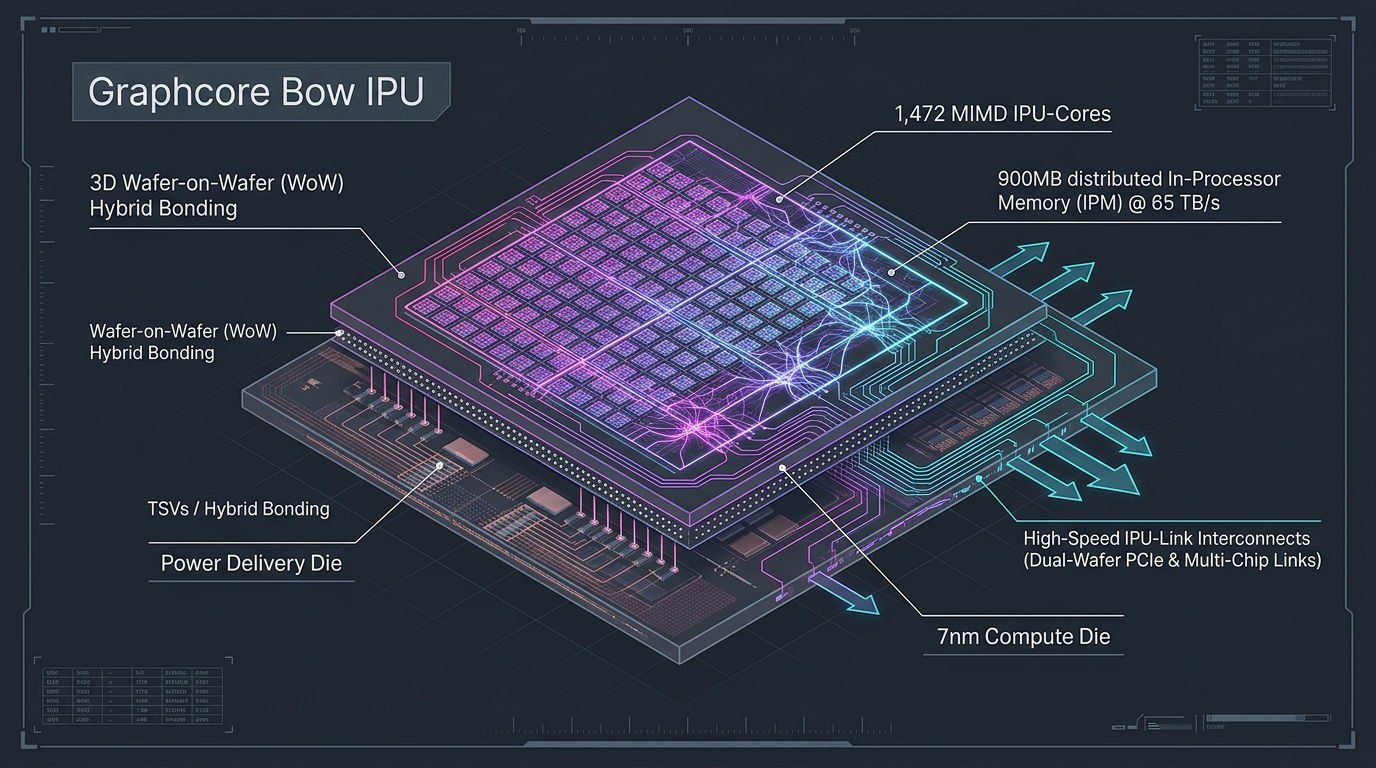
To eliminate the fundamental contradictions of SIMT execution, DRAM latency, and network jitter, Graphcore designed the Intelligence Processing Unit. With the release of the Bow IPU accelerator, Graphcore introduced the commercial semiconductor industry to 3D Wafer-on-Wafer (WoW) hybrid bonding, developed in close architectural collaboration with Taiwan Semiconductor Manufacturing Company.
The Bow IPU abandons the historical compromise of pairing processors with external commodity DRAM. Instead, it places the entire operational dataset directly on-chip within an ultra-wide 900 megabyte In-Processor Memory (IPM) static random-access memory array, delivering sixty-five terabytes per second of sustained internal memory bandwidth.
To power this massive computational substrate without suffering from thermal throttling or destructive supply voltage droop, the Bow IPU leverages vertical three-dimensional silicon stacking:
+----------------------------------------------------------------------------------------------------+
| GRAPHCORE BOW IPU: 3D WAFER-ON-WAFER (WoW) SILICON CROSS-SECTION                                   |
+----------------------------------------------------------------------------------------------------+
|                                                                                                    |
|    +------------------------------------------------------------------------------------------+    |
|    | TOP WAFER: Active 7nm Compute Die (Colossus IPU Architecture)                            |    |
|    | - 1,472 Independent MIMD Processing Cores (8,832 Hardware Worker Threads)                |    |
|    | - 900 MB On-Chip In-Processor Memory (SRAM) delivering 65 TB/s Local Bandwidth           |    |
|    | - 8 TB/s All-to-All On-Chip IPU-Exchange Crossbar Interconnect Fabric                    |    |
|    +------------------------------------------------------------------------------------------+    |
|                                   ||||||||||||||||||||||||||||||||||                               |
|    ==== HYBRID DIRECT BONDING: Dense Through-Silicon Vias (TSVs) at Sub-Micron Pitch ======    |
|                                   ||||||||||||||||||||||||||||||||||                               |
|    +------------------------------------------------------------------------------------------+    |
|    | BOTTOM WAFER: Deep-Trench Capacitor (DTC) Power Management Die                           |    |
|    | - Vertically Integrated Microscopic Capacitive Charge Reservoirs                         |    |
|    | - Sub-Nanosecond Transient Current Supply & Elimination of Power Distribution IR-Droop   |    |
|    | - Direct Structural Substrate & Power Grid Routing Layer                                 |    |
|    +------------------------------------------------------------------------------------------+    |
|                                                                                                    |
+----------------------------------------------------------------------------------------------------+ 1. TSMC 3D Wafer-on-Wafer Hybrid Bonding Mechanics
The foundational breakthrough of the Bow IPU lies in its manufacturing methodology. Rather than connecting distinct packaged dies across a shared silicon interposer as seen in 2.5D chiplet packaging, TSMC bonds two complete three-hundred-millimeter wafers face-to-face prior to singulation into individual processor chips:
- Wafer-Level Die Alignment: The bottom wafer is engineered with specialized power delivery circuits containing millions of integrated Deep-Trench Capacitors. The top wafer contains the complete seven-nanometer Colossus compute architecture, comprising 1,472 processor cores, memory banks, and exchange fabrics.
- Direct Copper-to-Copper Bonding: The two wafers are joined at the atomic level using hybrid bonding. Through-Silicon Vias connect the power management circuits of the bottom die directly into the transistors of the active compute die at sub-micron pitches.
- Thermal and Electrical Continuity: This face-to-face bonding eliminates the parasitic inductance and resistance inherent in traditional micro-bump packaging, creating an electrically unified monolithic silicon block with superior thermal dissipation properties.
2. Deep-Trench Capacitors and Dynamic IR-Drop Elimination
High-performance processors operating at gigahertz frequencies experience extreme transient power fluctuations. When thousands of arithmetic units simultaneously transition from idle states to dense matrix multiply-accumulate operations, current draw spikes across nanosecond intervals. In traditional packaging, the resistance of power delivery tracks causes an instantaneous voltage drop known as IR-drop:
- To safeguard against timing faults caused by IR-drop, conventional processors must either insert artificial clock throttling cycles or increase nominal supply voltage, severely compromising energy efficiency.
- The Bow IPU’s integrated bottom wafer acts as an instantaneous capacitive reservoir positioned mere micrometers from the arithmetic execution pipelines. When compute loads surge, the Deep-Trench Capacitors discharge current instantaneously, buffering the transient spike and smoothing the power supply.
- By virtually eliminating IR-drop, the Bow IPU achieves a forty percent increase in clock frequency (up to 1.85 GHz) and a sixteen percent improvement in power efficiency compared to previous generations, operating within an identical thermal footprint and power envelope.
3. True MIMD Architectural Autonomy
Rather than organizing execution around lock-step SIMT warps, the Bow IPU implements a genuine Multiple Instruction, Multiple Data (MIMD) architecture:
- Each of the 1,472 IPU-Cores functions as a fully independent computer processor with its own program counter, instruction fetch unit, arithmetic pipeline, and local memory bank.
- A core executing branch A experiences zero coupling or stalling when neighboring cores execute branch B, branch C, or recursive tree operations.
- This execution autonomy unlocks unprecedented performance on irregular sparse workloads, dynamic graph algorithms, and fine-grained agent loops.
Deep Architectural Analysis of the Bow IPU Subsystems
To understand how the Bow IPU delivers sustained computational efficiency across complex artificial intelligence models, we must examine its internal pipeline, memory hierarchies, synchronization primitives, and cluster scale-out fabrics.
+----------------------------------------------------------------------------------------------------+
| DETAILED ARCHITECTURAL BLOCK DIAGRAM: GRAPHCORE BOW IPU MICROARCHITECTURE                          |
+----------------------------------------------------------------------------------------------------+
|                                                                                                    |
|  +----------------------------------------------------------------------------------------------+  |
|  | 1,472 INDEPENDENT MIMD IPU-CORES (8,832 CONCURRENT HARDWARE EXECUTION THREADS)               |  |
|  |                                                                                              |  |
|  |  +-------------------------+  +-------------------------+     +-------------------------+    |  |
|  |  | Core 0 (Tile 0)         |  | Core 1 (Tile 1)         |     | Core 1471 (Tile 1471)   |    |  |
|  |  | - 6-Thread Barrel Pipe  |  | - 6-Thread Barrel Pipe  |     | - 6-Thread Barrel Pipe  |    |  |
|  |  | - 624 KB Local SRAM     |  | - 624 KB Local SRAM     | ... | - 624 KB Local SRAM     |    |  |
|  |  | - FP16/FP32 AMP Units   |  | - FP16/FP32 AMP Units   |     | - FP16/FP32 AMP Units   |    |  |
|  |  | - Stochastic Rounding   |  | - Stochastic Rounding   |     | - Stochastic Rounding   |    |  |
|  |  +-------------------------+  +-------------------------+     +-------------------------+    |  |
|  +----------------------------------------------------------------------------------------------+  |
|                                                ^                                                   |
|                                                | (Zero-Collision Compile-Time Routing)             |
|                                                v                                                   |
|  +----------------------------------------------------------------------------------------------+  |
|  | ON-CHIP IPU-EXCHANGE INTERCONNECT FABRIC (8.0 TB/s Sustained All-to-All Crossbar Bandwidth)   |  |
|  | - Fully non-blocking crossbar interconnecting all 1,472 tiles                               |  |
|  | - Deterministic hardware synchronization barrier: Sub-50ns latency resolution                |  |
|  +----------------------------------------------------------------------------------------------+  |
|                                                ^                                                   |
|                                                | (Inter-Socket Scale-Out)                          |
|                                                v                                                   |
|  +----------------------------------------------------------------------------------------------+  |
|  | MULTI-CHIP SCALE-OUT SUBSYSTEM: IPU-LINK INTERFACE (320 GB/s Bi-Directional Bandwidth)      |  |
|  | - Connects Bow IPUs into Bow-2000 chassis, Bow Pod16, Bow Pod64, and Bow Pod256 clusters     |  |
|  +----------------------------------------------------------------------------------------------+  |
|                                                                                                    |
+----------------------------------------------------------------------------------------------------+ 1. The 1,472 MIMD Processing Tiles and Hardware Barrel Multithreading
The foundational unit of the Bow IPU is the Tile. A single Bow IPU integrates exactly 1,472 tiles laid out across the physical silicon die:
- Core Execution Resources: Each tile contains an independent 64-bit superscalar processor core capable of executing control instructions, address arithmetic, and floating-point vector calculations.
- Accumulating Matrix Product Units: Integrated within each core is a dedicated Accumulating Matrix Product vector math unit capable of performing sixty-four mixed-precision FP16 operations per clock cycle with full FP32 accumulation.
- Six-Thread Barrel Processing: To hide memory access latencies without complex, power-hungry speculative branch prediction hardware, each core implements hardware multithreading supporting six concurrent execution contexts. The pipeline rotates strictly cycle-by-cycle between active threads in a barrel fashion. When thread zero issues an instruction reading from local SRAM, threads one through five execute consecutively, ensuring that thread zero’s memory operand is ready without pipeline stalls. Across the 1,472 cores, a single Bow IPU maintains 8,832 active hardware threads executing instructions simultaneously.
- Hardware Stochastic Rounding: In deep learning training, casting floating-point values from high precision to low precision introduces systematic statistical bias, often causing training divergence in small gradient ranges. Graphcore implements hardware-level stochastic rounding directly in the arithmetic execution logic. Rather than truncating or rounding to nearest, floating-point numbers are rounded up or down probabilistically proportional to their proximity to adjacent representable values. This allows networks to train stably using FP16 without requiring loss scaling or FP32 master weights.
2. In-Processor Memory: 900 MB On-Chip SRAM at 65 TB/s
Traditional accelerators use small on-chip caches (typically 40 MB to 60 MB of L2/L3 cache) backed by large off-chip DRAM. The Bow IPU overturns this architecture by eliminating off-chip DRAM entirely from the execution path:
- Distributed Local Storage: The 900 megabytes of high-speed SRAM are evenly partitioned across all 1,472 tiles, granting each core exactly 624 kilobytes of dedicated local memory.
- Zero-Latency Register Access: Because the memory is located immediately adjacent to the execution units on the active silicon die, cores access their local SRAM with single-cycle or dual-cycle latencies, completely bypassing cache hierarchy misses, tag lookups, and cache line invalidations.
- Aggregate Bandwidth: With 1,472 cores reading and writing to their local memory banks in parallel at 1.85 GHz, the aggregate memory throughput reaches an astonishing 65 terabytes per second, roughly twenty times faster than the external HBM3 subsystems used in state-of-the-art GPUs.
3. Bulk Synchronous Parallelism and the IPU-Exchange Crossbar
To coordinate computation and data exchange across 1,472 independent cores without suffering from deadlocks or packet contention, the Bow IPU adopts the Bulk Synchronous Parallel (BSP) computational model:
- Three-Phase Supersteps: Computation proceeds through repeated supersteps composed of three distinct phases:
- Compute Phase: Cores execute local arithmetic independently on their 624 KB memory slice. No inter-core communication occurs during this phase. Cores can branch, iterate, and compute at variable speeds.
- Sync Barrier: Once a core completes its compute phase, it signals hardware readiness and enters a synchronization barrier. Specialized on-chip hardware evaluates the global barrier across all 1,472 cores in under fifty nanoseconds.
- Exchange Phase: Once all cores reach the barrier, inter-core data exchange begins. Data is transported across the IPU-Exchange crossbar, a non-blocking internal switching network delivering eight terabytes per second of all-to-all bandwidth.
- Static Compile-Time Routing: The Poplar compiler analyzes the full neural network graph and schedules every single data packet’s transmission path and clock cycle prior to execution. Because the exact arrival and departure times of every packet are deterministically pre-calculated, the IPU-Exchange requires zero dynamic arbitration buffers, zero flow-control packets, and produces zero runtime packet collisions.
+----------------------------------------------------------------------------------------------------+
| BULK SYNCHRONOUS PARALLEL (BSP) EXECUTION LIFECYCLE                                                |
+----------------------------------------------------------------------------------------------------+
|                                                                                                    |
|  SUPERSTEP N:                                                                                      |
|  +----------------------------------------------------------------------------------------------+  |
|  | COMPUTE PHASE: 1,472 Cores run independently on 624KB local SRAM. Zero inter-core traffic.  |  |
|  | [Core 0: Active]   [Core 1: Active]   ...   [Core 1470: Active]   [Core 1471: Active]        |  |
|  +----------------------------------------------------------------------------------------------+  |
|                                                |                                                   |
|                                                v                                                   |
|  +----------------------------------------------------------------------------------------------+  |
|  | HARDWARE SYNCHRONIZATION BARRIER: Deterministic global handshake resolved in <50 nanoseconds  |  |
|  +----------------------------------------------------------------------------------------------+  |
|                                                |                                                   |
|                                                v                                                   |
|  +----------------------------------------------------------------------------------------------+  |
|  | EXCHANGE PHASE: IPU-Exchange crossbar moves data at 8.0 TB/s. Zero runtime packet collisions.|  |
|  | Pre-scheduled static routing paths guarantee deterministic transmission cycles.               |  |
|  +----------------------------------------------------------------------------------------------+  |
|                                                                                                    |
+----------------------------------------------------------------------------------------------------+ 4. Multi-Chip Scaling via IPU-Link
To scale workloads beyond a single processor, the Bow IPU features ten specialized IPU-Link high-speed inter-chip interfaces delivering 320 gigabytes per second of bi-directional off-chip bandwidth:
- Bow-2000 System Architecture: The standard building block is the Bow-2000, a 1U chassis containing four Bow IPU processors (5,888 MIMD cores, 3.6 GB of SRAM at 260 TB/s, delivering 1.4 PFLOPS of mixed-precision compute).
- Bow Pod Form Factors: IPU-Links connect Bow-2000 machines into integrated rack-scale systems:
- Bow Pod16: Four Bow-2000 units (16 IPUs) interconnected in a 2D mesh, offering 14.4 GB of on-chip SRAM and 5.6 PFLOPS compute.
- Bow Pod64: Sixteen Bow-2000 units (64 IPUs) linked with ultra-low latency routing for enterprise model training.
- Bow Pod256: Sixty-four Bow-2000 units (256 IPUs) delivering over 89.6 PFLOPS of compute and 230 GB of aggregate on-chip SRAM operating as a single unified BSP accelerator.
Hands-On Poplar SDK and PopTorch Implementation Guide
Developing software for the Graphcore Bow IPU differs significantly from writing standard CUDA kernels. Graphcore’s software stack, the Poplar SDK, operates on complete computational computational graphs, mapping neural network layers directly into tiles, vertices, and exchange schedules.
+----------------------------------------------------------------------------------------------------+
| POPLAR SDK SOFTWARE STACK ARCHITECTURE                                                             |
+----------------------------------------------------------------------------------------------------+
| USER INTERFACE: PyTorch (PopTorch), TensorFlow, ONNX, JAX                                          |
+----------------------------------------------------------------------------------------------------+
                                         |
+----------------------------------------------------------------------------------------------------+
| POPLAR GRAPH ENGINE & PopART: Graph Optimization, Tile Partitioning & BSP Scheduling               |
| - Decomposes computational graphs into fine-grained compute sets and static exchange patterns       |
+----------------------------------------------------------------------------------------------------+
                                         |
+----------------------------------------------------------------------------------------------------+
| COMPILER BACKEND: Native IPU Assembly Generation & Deterministic Memory Allocator (624KB/tile)     |
+----------------------------------------------------------------------------------------------------+
                                         |
+----------------------------------------------------------------------------------------------------+
| PHYSICAL HARDWARE: Graphcore Bow IPU (3D Wafer-on-Wafer Silicon via TSV Hybrid Direct Bonding)     |
+----------------------------------------------------------------------------------------------------+ 1. Training a Sparse Graph Neural Network with PopTorch
Graph Neural Networks represent a prime use case where standard GPUs experience severe warp serialization due to irregular node degree distributions. Below is a comprehensive Python implementation using poptorch, compiling a Graph Convolutional Network (GCN) layer for execution across Bow IPU tiles:
# ============================================================================
# File: train_gnn_poptorch.py
# Description: Graph Convolutional Network Training on Graphcore Bow IPU
# Hardware: Graphcore Bow-2000 (4x Bow IPU Accelerators)
# Software: Poplar SDK 3.x / PopTorch / PyTorch 2.x
# ============================================================================

import torch
import torch.nn as nn
import poptorch

class IPUSparseGCNLayer(nn.Module):
    # Graph Convolutional Layer mapped to Graphcore Bow IPU MIMD Cores.
    # Leverages 900MB on-chip In-Processor Memory for sub-nanosecond message passing.
    def __init__(self, in_features: int, out_features: int):
        super().__init__()
        self.in_features = in_features
        self.out_features = out_features
        # Initialize weight matrix on IPU tile memory
        self.weight = nn.Parameter(torch.randn(in_features, out_features) * 0.02)
        self.bias = nn.Parameter(torch.zeros(out_features))
        self.activation = nn.GELU()

    def forward(self, node_features: torch.Tensor, adjacency_matrix: torch.Tensor) -> torch.Tensor:
        # Step 1: Linear Transformation using IPU AMP Matrix Units
        # Tensor Shape: [N, in_features] x [in_features, out_features] -> [N, out_features]
        support = torch.matmul(node_features, self.weight)

        # Step 2: Sparse Message Passing across the On-Chip IPU-Exchange
        # Because each of the 1,472 cores executes independently (MIMD),
        # variable degree node distributions process without warp divergence!
        output = torch.matmul(adjacency_matrix, support) + self.bias
        return self.activation(output)

class IPUTrainingWrapper(nn.Module):
    # Wraps the model and loss function into a single computational graph
    # optimized for Poplar compile-time BSP scheduling.
    def __init__(self, model: nn.Module, loss_fn: nn.Module):
        super().__init__()
        self.model = model
        self.loss_fn = loss_fn

    def forward(self, node_features, adjacency_matrix, targets):
        predictions = self.model(node_features, adjacency_matrix)
        loss = self.loss_fn(predictions, targets)
        return poptorch.identity_loss(loss, reduction="mean")

def configure_bow_ipu_options() -> poptorch.Options:
    # Configures hardware-specific execution parameters for Bow IPU
    opts = poptorch.Options()

    # 1. Enable hardware stochastic rounding for FP16 training stability
    opts.Precision.enableStochasticRounding(True)

    # 2. Replicate model across multiple IPUs if available (e.g., Bow-2000 4x IPUs)
    opts.replicationFactor(1)

    # 3. Optimize memory allocation across 1,472 tiles (targeting 624 KB per core)
    opts.setExecutionStrategy(poptorch.ShardedExecution())
    opts.anchorTensor("loss", "mean")

    # 4. Enable Poplar compiler optimization level
    opts.setEngineOption({"opt.internalExchangeOptimization": "true"})
    return opts

def run_bow_ipu_gnn_training():
    print("Initializing Graphcore Bow IPU GNN Training Session...")

    # Model Hyperparameters
    NUM_NODES = 4096
    FEATURE_DIM = 128
    HIDDEN_DIM = 256
    NUM_CLASSES = 16

    # Construct PyTorch Network
    class GNNModel(nn.Module):
        def __init__(self):
            super().__init__()
            self.layer1 = IPUSparseGCNLayer(FEATURE_DIM, HIDDEN_DIM)
            self.layer2 = IPUSparseGCNLayer(HIDDEN_DIM, NUM_CLASSES)

        def forward(self, x, adj):
            h = self.layer1(x, adj)
            out = self.layer2(h, adj)
            return out

    base_model = GNNModel()
    loss_function = nn.CrossEntropyLoss()
    training_model = IPUTrainingWrapper(base_model, loss_function)

    # Configure PopTorch Options for Bow IPU
    opts = configure_bow_ipu_options()
    optimizer = poptorch.optim.AdamW(training_model.parameters(), lr=1e-3, weight_decay=1e-4)

    # Wrap model into PopTorch Training Engine (triggers Poplar graph compilation)
    poptorch_model = poptorch.trainingModel(training_model, options=opts, optimizer=optimizer)

    # Generate synthetic graph tensors resident in 900MB IPM SRAM
    node_features = torch.randn(NUM_NODES, FEATURE_DIM)
    adjacency = torch.randn(NUM_NODES, NUM_NODES)
    labels = torch.randint(0, NUM_CLASSES, (NUM_NODES,))

    print("Compiling Poplar Graph Engine binary for 1,472 MIMD IPU-Cores...")
    for epoch in range(5):
        loss = poptorch_model(node_features, adjacency, labels)
        print(f"Epoch {epoch + 1:02d} | CrossEntropy Loss: {loss:.4f}")

    # Explicitly release physical hardware accelerator handles
    poptorch_model.destroy()
    print("Graphcore Bow IPU GNN Training Session successfully completed.")

if __name__ == "__main__":
run_bow_ipu_gnn_training() 2. Monitoring Tile Balance with PopVision Graph Analyser
Because the Bow IPU relies on 1,472 distributed memory slices, unbalanced memory allocations can cause an individual tile to exceed its 624 KB SRAM capacity. Developers utilize the PopVision Graph Analyser to audit tile balancing:
# ============================================================================
# Script: profile_bow_ipu.sh
# Description: Generate and inspect Poplar execution traces with PopVision
# ============================================================================

# Enable Poplar Graph Engine Profiling Environment Flags
export POPLAR_ENGINE_OPTIONS='{
  "autoReport.all": "true",
  "autoReport.directory": "./profiler_reports",
  "debug.instrumentCompute": "true"
}'

# Execute PopTorch script on physical hardware
python3 train_gnn_poptorch.py

# Inspect generated report files using PopVision GUI or CLI
# Key Metrics to Audit:
# 1. Tile Memory Footprint: Verify all 1,472 cores remain below 620 KB (<98% capacity).
# 2. BSP Ratio: Verify compute phase accounts for >80% of total cycle execution time.
# 3. Sync Barrier Delay: Ensure hardware sync latency remains under 50 nanoseconds. Architectural Comparison: Graphcore Bow IPU vs. NVIDIA H100 SXM5
To understand the strategic trade-offs of the Bow IPU architecture, we examine a rigorous head-to-head comparison against the premier dense computing accelerator, the NVIDIA H100 SXM5:
+----------------------------------------------------------------------------------------------------+
| HARDWARE SPECIFICATIONS COMPARISON (SINGLE ACCELERATOR MODULE)                                     |
+----------------------------------------------------------------------------------------------------+
| Architectural Metric          | NVIDIA H100 SXM5       | Graphcore Bow IPU (Colossus WoW)          |
+-------------------------------+------------------------+-------------------------------------------+
| Manufacturing Technology      | TSMC 4N Custom 5nm     | TSMC 3D Wafer-on-Wafer (7nm + Power Die)  |
| Execution Paradigm            | SIMT (32-Thread Warps) | True MIMD (1,472 Independent Processor Cores)|
| Total Parallel Threads        | ~4,224 Active Threads  | 8,832 Hardware Worker Threads             |
| On-Chip High-Speed Memory     | 50 MB L2 Cache         | 900 MB In-Processor Memory (IPM SRAM)     |
| Internal Memory Bandwidth     | 3.35 TB/s (HBM3)       | 65.0 TB/s (In-Processor SRAM)             |
| External Memory Subsystem     | 80 GB HBM3             | None (Pure On-Chip) / Host Streaming DRAM |
| Floating-Point Precision      | FP8, FP16, BF16, TF32  | FP16, FP32 with Stochastic Rounding       |
| Peak Mixed-Precision Compute  | 989.5 TFLOPS (BF16)    | 350.0 TFLOPS (Mixed FP16/FP32)            |
| Inter-Chip Networking Fabric  | NVLink 4 (900 GB/s)    | IPU-Link (320 GB/s)                       |
| Synchronization Protocol      | Dynamic Warp Locks     | Deterministic Bulk Synchronous (BSP)      |
| Best-Fit Workload Focus       | Dense LLM GEMMs        | Graph Neural Networks, MCMC, Sparse Models|
+----------------------------------------------------------------------------------------------------+ 1. Detailed Metric Evaluations
Evaluating the structural implications of these divergent design philosophies reveals clear operational boundaries:
2. True MIMD Processing vs. SIMT Warp Divergence
- Algorithmic Freedom: On the H100, if threads within a warp diverge on conditional branches, execution serializes. On the Bow IPU, all 1,472 cores execute completely independent instruction streams with zero branch serialization. This makes Bow IPU fundamentally superior for non-uniform data structures, dynamic graph traversals, and fine-grained agent reasoning loops.
3. On-Chip SRAM Bandwidth (65 TB/s) vs. External HBM3 (3.35 TB/s)
- Twenty-Fold Memory Advantage: While the H100 achieves 3.35 TB/s across an external 2.5D CoWoS HBM interface, the Bow IPU delivers 65 TB/s of internal memory bandwidth directly across its 900 MB In-Processor Memory. For workloads that fit resident in SRAM (such as graph models, embeddings, small language models, or image processing filters), Bow IPU executes arithmetic with near-zero latency and minimal energy dissipation.
4. Deterministic BSP Synchronization vs. Dynamic GPU Jitter
- Elimination of Tail Latency: While large GPU clusters suffer from runtime network tail latencies and non-deterministic kernel race conditions, Graphcore’s Bulk Synchronous Parallel model coordinates data exchange with sub-50ns synchronization barriers and compile-time pre-routed communications, guaranteeing cycle-accurate determinism.
Production Deployment & Enterprise Scaling
Deploying Graphcore Bow IPUs in enterprise datacenter environments requires understanding system packaging, host orchestration, memory streaming pipelines, and strategic workload mapping.
1. Bow-2000 System Integration and Rack Infrastructure
In commercial datacenters, Bow IPUs are packaged into Bow-2000 1U chassis units:
- Each Bow-2000 integrates four Bow IPU processors, delivering 1.4 PFLOPS of mixed-precision compute, 3.6 GB of SRAM at 260 TB/s, and eight IPU-Links.
- The system pairs with dual AMD EPYC or Intel Xeon host servers connected over high-speed PCIe Gen 4 links.
- Dual redundant 2000W power supplies and high-velocity cooling fans manage the thermal dissipation of the vertically bonded 3D silicon, maintaining operating junction temperatures below seventy-five degrees Celsius.
2. Streaming Host Memory via Poplar Remote Buffers
Because a single Bow IPU contains 900 MB of SRAM, models with parameter footprints exceeding on-chip memory utilize Poplar’s Remote Buffers feature:
- Weights and optimizer states are stored in host system DDR5 RAM or dedicated streaming NVMe storage.
- During the BSP execution cycle, Poplar streams parameters dynamically into local 624 KB tile memories across PCIe Gen 4 lanes ahead of compute supersteps, overlapping communication with calculation.
- This hybrid pipeline enables Bow clusters to train large-scale vision and transformer models that exceed physical on-chip SRAM capacity while maintaining high compute utilization.
3. Decision Matrix: When to Choose Graphcore Bow IPU vs. GPUs
Enterprise architecture teams should apply this structured decision framework when evaluating hardware selection:
| Workload Characteristic | Preferred Architecture | Rationale & Operational Advantage |
|---|---|---|
| Dense LLM Pre-Training (70B+ Params) | NVIDIA GPU (H100 / B200) | Dense GEMM tensor cores and 80GB-192GB HBM capacity accommodate enormous weight matrices natively. |
| Graph Neural Networks (GNNs) | Graphcore Bow IPU | 1,472 independent MIMD cores traverse irregular node neighborhoods without warp divergence stalls. |
| Sparse Mixture-of-Experts (MoE) | Graphcore Bow IPU | Fine-grained routing tokens distribute across tiles without serializing execution threads. |
| Probabilistic MCMC & Bayesian Networks | Graphcore Bow IPU | Independent execution streams handle asynchronous sampling and dynamic branch paths natively. |
| Sub-Millisecond Inference Serving | Graphcore Bow IPU | 65 TB/s SRAM bandwidth eliminates DRAM access latency, achieving microsecond-scale response times. |
| Dynamic Document & Web Parsing | Graphcore Bow IPU | Complex tree structures and irregular AST evaluations execute without lock-step thread penalties. |
By mastering the 3D Wafer-on-Wafer silicon innovations, MIMD microarchitecture, and Poplar graph programming model of the Graphcore Bow IPU, engineering teams can unlock unprecedented throughput for the next frontier of irregular, sparse, and graph-native artificial intelligence workloads.