Google TPU v6e Guide: Trillium Architecture & XLA Serving
The Datacenter Power and Matrix Compute Bottleneck
In modern hyperscale cloud computing, automated agentic research platforms, and enterprise data extraction engines powered by AI Fetchly, computational infrastructure is bound by severe thermodynamics and silicon scaling walls. Whether deploying high-concurrency LLM inference nodes, executing continuous web harvesting operations via automated web scraping, or orchestrating enterprise data pipelines through real-time data ingestion, datacenter operators face soaring electricity consumption, thermal dissipation barriers, and rising hardware costs.
Over the past decade, general-purpose graphics processing units (GPUs) became the default accelerator for machine learning. However, because graphics hardware evolved from rasterization and pixel shaders, traditional GPUs carry substantial architectural baggage that degrades power efficiency and execution determinism in production:
1. Complex Control Logic and Instruction Scheduling Overhead
Modern GPUs rely on dynamic hardware schedulers, out-of-order execution buffers, and large register files to manage thousands of active threads (SIMT). While this flexibility accommodates non-uniform scientific simulations, it introduces significant inefficiencies for deep neural networks:
- Neural network architectures—such as transformers, diffusion models, and recommendation graphs—consist predominantly of dense matrix multiplications and static tensor contractions whose execution graphs are fully known in advance.
- Managing thread warps, handling branch divergence, and arbitrating memory cache coherency dynamically in silicon burns up to 30% to 40% of the chip’s electrical power before any floating-point arithmetic takes place.
- Hardware-level dynamic scheduling creates non-deterministic latency jitter, complicating synchronized collective communications across large distributed clusters.
- Because instruction issue and register file read stages consume massive power, GPUs require aggressive active liquid cooling and complex cooling distribution units (CDUs) to avoid thermal throttling.
Systolic Array vs. Traditional GPU Execution Model:
+------------------------------------------------------------------------------------+
| TRADITIONAL GPU (SIMT): Thread Schedulers & Repeated Register File Trips           |
+------------------------------------------------------------------------------------+
| [Registers / Cache] <---> [Dynamic Scheduler] <---> [ALU / Tensor Core]            |
| - High dynamic instruction fetch & decode power overhead                           |
| - Data repeatedly shuttled back and forth from register files between operations   |
| - Unpredictable memory access latency across divergent thread warps                |
+------------------------------------------------------------------------------------+
| GOOGLE TPU (SYSTOLIC ARRAY): 2D Spatial Data Streaming Without Register Stalls     |
+------------------------------------------------------------------------------------+
| Input Activations ===> [PE] -> [PE] -> [PE] -> [PE] ===> Output Accumulator        |
|                         |       |       |       |                                  |
| Weights Pre-loaded    [PE] -> [PE] -> [PE] -> [PE]                                 |
| - Zero dynamic instruction overhead; data flows continuously across adjacent ALUs  |
| - 67% reduction in energy consumption per floating-point operation                 |
+------------------------------------------------------------------------------------+ 2. The 128x128 Systolic Array Saturation Barrier
In earlier Tensor Processing Unit generations (such as TPU v2 through TPU v5e), Google utilized Matrix Multiply Units (MXUs) structured as 128x128 systolic arrays:
- A 128x128 systolic array performs 16,384 multiply-accumulate (MAC) operations per cycle.
- While revolutionary when first introduced, the rapid explosion of foundation model parameter dimensions (hidden dimensions exceeding 4,096 to 12,288 elements) meant that 128x128 tiles required hundreds of sequential sub-block iterations to process a single linear projection.
- Feeding smaller systolic arrays requires higher memory read frequencies, putting undue pressure on memory controllers and limiting arithmetic intensity.
- As foundation model batch sizes grow, small systolic tiles spend an excessive percentage of execution cycles performing setup and draining phases relative to steady-state compute.
3. The Embedding and Recommendation Memory Penalty
Modern enterprise AI workloads are not limited to autoregressive language models; they are heavily driven by massive recommendation systems and deep learning ranking models (DLRM). Recommendation models process embedding tables containing billions of sparse categorical parameters:
- Sparse embedding lookups feature irregular, non-coalesced memory access patterns that leave matrix multiplication engines completely idle while waiting on high-latency memory fetches.
- Processing sparse embeddings on standard GPU tensor cores or dense TPU MXUs results in single-digit hardware utilization, forcing cloud providers to waste expensive compute silicon on simple memory lookups.
- Standard general-purpose accelerators lack dedicated memory gathering pipelines, causing severe memory bus contention between dense activations and sparse categorical indices.
The Trillium Leap: Google Cloud TPU v6e Architecture
To conquer these scaling hurdles and provide an ultra-efficient computing foundation for the generative AI era, Google engineered its sixth-generation custom AI accelerator: Cloud TPU v6e, codenamed Trillium.
Announced as part of Google Cloud’s AI Hypercomputer architecture, Trillium is designed specifically to deliver optimal cost-performance and energy efficiency for both training and serving frontier foundation models (including Google’s Gemini, Gemma, and enterprise open weights).
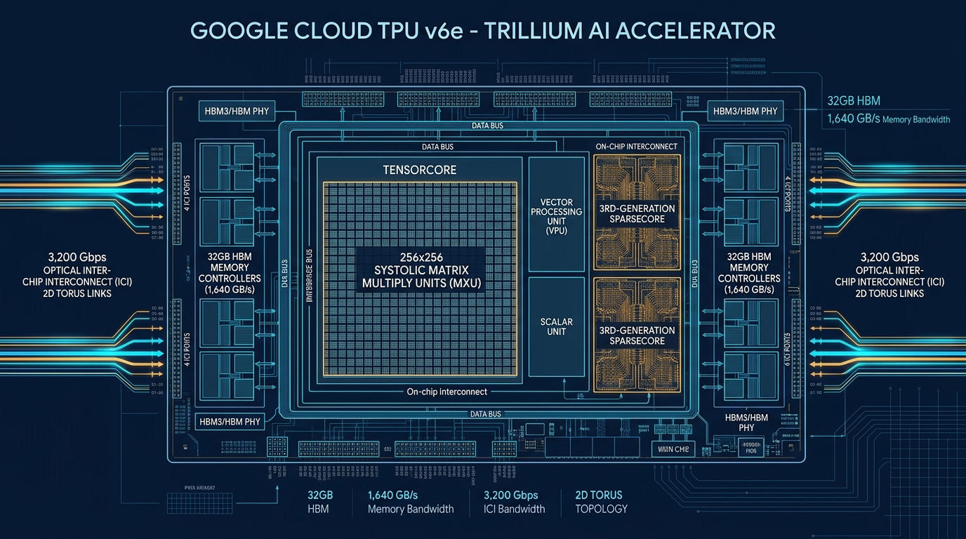
Google Cloud TPU v6e (Trillium) Silicon Floorplan:
+------------------------------------------------------------------------------------+
| GOOGLE CLOUD TPU v6e (TRILLIUM) ACCELERATOR ARCHITECTURE                           |
+------------------------------------------------------------------------------------+
|                                                                                    |
|  +------------------------------------------------------------------------------+  |
|  | DUAL TENSORCORE COMPUTING ENGINES                                            |  |
|  |                                                                              |  |
|  |  +-------------------------------------+  +-------------------------------+  |  |
|  |  | 256x256 Systolic Matrix Multiply    |  | Vector Processing Unit (VPU)  |  |  |
|  |  | Unit (MXU) - 65,536 MACs / Cycle    |  | - Softmax, LayerNorm, GELU    |  |  |
|  |  | - Native BF16 Inputs / FP32 Acc     |  | - Element-wise Math, RMSNorm  |  |  |
|  |  +-------------------------------------+  +-------------------------------+  |  |
|  |                                                                              |  |
|  |  +------------------------------------------------------------------------+  |  |
|  |  | Scalar Processing Unit & Control Logic Engine                          |  |  |
|  |  +------------------------------------------------------------------------+  |  |
|  +------------------------------------------------------------------------------+  |
|                                        ||                                          |
|  +------------------------------------------------------------------------------+  |
|  | THIRD-GENERATION SPARSECORE SUBSYSTEM                                        |  |
|  | - Dedicated hardware acceleration for DLRM embedding lookups & gather/scatter|  |
|  | - Ultra-high bandwidth atomic reductions & sparse vector hashing             |  |
|  +------------------------------------------------------------------------------+  |
|                                        ||                                          |
|  +----------------------------------+  +-----------------------------------------+  |
|  | 32 GB High-Bandwidth Memory HBM  |  | 3,200 Gbps Optical ICI Interconnect     |  |
|  | - 1,640 GB/s Sustained Bandwidth |  | - Native 2D Torus Topology (256 Chips)   |  |
|  +----------------------------------+  +-----------------------------------------+  |
+------------------------------------------------------------------------------------+ 1. 4.7x Compute Densification via 256x256 Systolic Arrays
The defining microarchitectural leap in Trillium is the expansion of its systolic matrix engine:
- 256x256 Systolic Array: Trillium quadruples the physical matrix multiply array dimensions from 128x128 to 256x256 multiply-accumulators.
- 65,536 MAC Operations per Cycle: Each MXU executes 65,536 mathematical operations every clock cycle, performing 4x more arithmetic operations per cycle than previous generations.
- Combined with architectural clock frequency advancements and optimized silicon lithography, Trillium delivers an impressive 4.7x increase in peak compute performance per chip compared to its predecessor, TPU v5e.
- This architectural expansion matches modern transformer projections perfectly: calculating attention query, key, and value matrices on 256-wide dimensions aligns with hardware tiles with zero zero-padding waste.
2. Doubled Memory Capacity and Bandwidth
To sustain high utilization across its massive 256x256 systolic arrays, Google doubled both memory density and memory interface bandwidth:
- 32 GB High-Bandwidth Memory (HBM): Doubles the on-chip capacity from 16 GB on v5e to 32 GB on v6e, accommodating larger batch sizes and longer KV cache contexts.
- 1,640 GB/s (1.64 TB/s) Memory Bandwidth: Doubles memory throughput, feeding activation tensors and model weights into the computing engines with minimal memory wait states.
- 3x Host DRAM Capacity: TPU v6e hosts feature tripled system memory capacity, speeding up dataset caching, tokenization pipelines, and host-to-device streaming.
3. Third-Generation SparseCore Acceleration
Trillium integrates Google’s third-generation SparseCore:
- A specialized hardware accelerator designed specifically to execute sparse, irregular operations: sparse embedding lookups, dynamic gather/scatter primitives, and multi-hot categorical feature reductions.
- Operating alongside the dense MXU, SparseCore offloads embedding transformations from the primary tensor compute engines, accelerating ranking models (DLRM) and Mixture-of-Experts (MoE) token routing gates by up to 2x compared to TPU v5e.
- SparseCore features its own dedicated SRAM buffers and memory channels, preventing sparse memory access streams from polluting or stalling the primary HBM channels serving the matrix engines.
4. 67% Greater Energy Efficiency
Datacenter operational costs are governed by energy expenditure per token. Trillium operates with 67% greater energy efficiency (performance-per-watt) than TPU v5e, allowing hyperscalers to deploy larger compute clusters within fixed megawatt datacenter power caps.
Deep Dive: Trillium Microarchitecture, ICI Pods, and the XLA Compiler
To appreciate how Google Cloud TPU v6e operates, we examine its three foundational pillars: the systolic compute core, the Inter-Chip Interconnect (ICI) optical network fabric, and the Accelerated Linear Algebra (XLA) optimizing compiler.
1. The TensorCore: MXU, VPU, and Scalar Units
Each TPU v6e chip contains high-performance TensorCores consisting of:
- Matrix Multiply Unit (MXU): Operates on a 256x256 grid of processing elements (PEs). In a systolic array, data flows rhythmically across adjacent processing elements in lockstep:
- Inputs (activations) stream in from the left edges.
- Model weights are stationary, pre-loaded into the processing elements.
- Partial sums accumulate downwards through the array.
- Inputs are BFLOAT16 (16-bit brain floating point), while accumulations are computed in full FP32 precision to preserve mathematical stability during deep gradient descent and long-sequence self-attention.
- Vector Processing Unit (VPU): Dedicated SIMD vector engine responsible for operations that cannot be formulated as pure matrix multiplications: activation functions (GELU, SwiGLU, SiLU), LayerNorm, RMSNorm, softmax reductions, and rotary positional embeddings (RoPE).
- Scalar Unit: Manages program counter sequencing, conditional branching, memory address calculations, and loop counters.
Detailed 256x256 Systolic Array Dataflow:
+------------------------------------------------------------------------------------+
| 256x256 SYSTOLIC ARRAY MATRIX MULTIPLY UNIT (MXU)                                  |
+------------------------------------------------------------------------------------+
|                                                                                    |
|                  Weight Stationary Matrix Elements Pre-Loaded In PEs               |
|                                                                                    |
|   Activation         PE[0,0]    --->    PE[0,1]    --->    PE[0,255]               |
|   Vector Stream       |                  |                  |                      |
|   (BFLOAT16)          v                  v                  v                      |
|   X0, X1, ... =====> PE[1,0]    --->    PE[1,1]    --->    PE[1,255]               |
|                       |                  |                  |                      |
|                       v                  v                  v                      |
|                      PE[255,0]  --->    PE[255,1]  --->    PE[255,255]             |
|                       |                  |                  |                      |
|                       v                  v                  v                      |
|                  ===================================================               |
|                  FP32 Partial Accumulator Registers (65,536 MACs / Cycle)          |
|                  ===================================================               |
|                                                                                    |
+------------------------------------------------------------------------------------+ 2. Microarchitectural Mechanics of SparseCore v3
Google’s SparseCore represents one of the most innovative domain-specific additions to modern accelerator hardware. While conventional accelerators treat sparse embedding lookups as general memory gather operations, SparseCore implements a dedicated dataflow pipeline:
- Pipelined Index Translation: Categorical feature indices (e.g., user IDs, search query tokens, video interaction tags) are parsed by dedicated address translation units that map sparse IDs directly to physical HBM memory addresses.
- Asynchronous Tile Prefetching: SparseCore features autonomous DMA engines that fetch sparse embedding rows into local on-chip scratchpad memory ahead of time, completely decoupling memory retrieval from matrix core execution.
- On-the-Fly Reduction ALU: Instead of loading embedding vectors into high-power vector units for pooling, SparseCore contains lightweight local ALUs that perform sum, average, and max pooling operations directly at the memory interface.
- MoE Token Routing Offloading: In Mixture-of-Experts foundation models, routing tokens to top-k expert neural networks requires sorting and routing millions of tokens dynamically. SparseCore accelerates expert gating calculations, ensuring that dense MXU tiles receive balanced token queues.
3. The 3,200 Gbps Inter-Chip Interconnect (ICI) 2D Torus Pod
Unlike traditional GPU clusters that require expensive external PCIe switches and InfiniBand network interface cards to connect servers, Google TPUs integrate dedicated optical network routers directly on the processor die:
- Inter-Chip Interconnect (ICI): Each Trillium chip features dedicated hardware ICI links providing 3,200 Gbps (3.2 Tbps) of bidirectional point-to-point bandwidth.
- 2D Torus Topology: Within a Cloud TPU v6e Pod, chips are wired in a two-dimensional wrap-around grid (2D torus). Every chip has direct physical optical links to its North, South, East, and West neighbors.
- Pod Scaling up to 256 Chips: A standard full TPU v6e Pod houses 256 chips, pooling 8,192 GB (8.19 TB) of HBM and delivering immense aggregate bisection bandwidth without passing through a single external top-of-rack Ethernet switch.
- Multislice Scaling: For mega-scale models requiring thousands of accelerators, Google links multiple pods together using its Jupiter optical datacenter network, utilizing Multislice technology to scale workloads across tens of thousands of TPU chips seamlessly.
Cloud TPU v6e 2D Torus Inter-Chip Interconnect (ICI) Pod Layout:
┌────────────────────────────────────────────────────────────────────────┐
│ TPU v6e 2D TORUS INTERCONNECT FABRIC (UP TO 256 CHIPS PER POD)         │
│                                                                        │
│   [TPU 0,0] <=== 3200 Gbps ===> [TPU 0,1] <=== 3200 Gbps ===> [TPU 0,X]│
│       ^                             ^                             ^    │
│       ||                            ||                            ||   │
│   [TPU 1,0] <=== 3200 Gbps ===> [TPU 1,1] <=== 3200 Gbps ===> [TPU 1,X]│
│       ^                             ^                             ^    │
│       ||                            ||                            ||   │
│   [TPU Y,0] <=== 3200 Gbps ===> [TPU Y,1] <=== 3200 Gbps ===> [TPU Y,X]│
│                                                                        │
│   - Direct point-to-point optical links; zero external switch latency  │
│   - Deterministic communication latency for All-Reduce & All-to-All    │
└────────────────────────────────────────────────────────────────────────┘ 4. The XLA Compiler: Whole-Graph Optimization and Kernel Fusion
The software engine powering Google TPUs is OpenXLA (Accelerated Linear Algebra). Unlike PyTorch on CUDA—which often executes kernels greedily one after another, writing intermediate tensors back to global memory—XLA compiles entire computational graphs into fused machine code:
- Kernel Fusion: XLA fuses sequences of linear layers, bias additions, layer normalizations, and activations into single execution kernels. Intermediate values remain held in local registers and on-chip scratchpad memory, completely eliminating trips to off-chip HBM.
- Memory Buffer Allocation: XLA statically schedules the exact physical memory address of every tensor across the entire lifetime of the model. Because memory allocation is planned ahead of time, TPUs suffer zero memory fragmentation and zero runtime garbage collection pauses.
- Automated Layout Optimization: XLA automatically transposes and tiles tensors to match the physical 256x256 dimensions of the Trillium systolic array.
- HLO Intermediate Representation: PyTorch and JAX models are translated into High-Level Optimizer (HLO) instructions, allowing backend compilers to apply target-specific vectorization, unrolling, and collective communication overlap automatically.
Concrete Implementation: JAX Model Training & vLLM Serving on TPU v6e
To illustrate how software interacts with Google Cloud TPU v6e hardware, we provide two complete, production-ready examples: distributed matrix computation in JAX and high-throughput LLM serving via vLLM on Google Kubernetes Engine (GKE).
1. Distributed Tensor Parallelism in JAX with jax.sharding
JAX is the native programming framework for TPUs, designed by Google DeepMind. Using JAX’s unified array sharding API (Mesh and NamedSharding), developers can shard multi-head attention layers across a TPU v6e pod with zero low-level MPI or NCCL calls:
# ============================================================================
# File: distributed_tpu_v6e_gemm.py
# Description: Multi-Device Matrix Sharding on Google Cloud TPU v6e Pods via JAX
# ============================================================================

import jax
import jax.numpy as jnp
from jax.sharding import Mesh, PartitionSpec as P, NamedSharding
import numpy as np

def run_distributed_tpu_v6e():
    # 1. Discover TPU v6e Hardware Devices
    devices = jax.devices()
    num_devices = len(devices)
    print(f"Discovered {num_devices} Cloud TPU v6e devices: {devices}")

    # 2. Establish 2D Device Mesh (Data Parallelism x Model Parallelism)
    # For an 8-chip slice, configure a 2x4 mesh
    mesh_shape = (2, num_devices // 2) if num_devices >= 4 else (1, num_devices)
    device_mesh = np.array(devices).reshape(mesh_shape)
    mesh = Mesh(device_mesh, axis_names=('data', 'model'))

    # 3. Define Matrix Dimensions Matching Trillium 256x256 MXU Tiling
    BATCH_SIZE = 4096
    HIDDEN_IN = 8192
    HIDDEN_OUT = 8192

    # 4. Define Named Sharding Specifications
    # Input Activations: Sharded along 'data' axis
    # Weight Matrix: Sharded along 'model' axis (Tensor Parallel Column Sharding)
    act_sharding = NamedSharding(mesh, P('data', None))
    weight_sharding = NamedSharding(mesh, P(None, 'model'))
    out_sharding = NamedSharding(mesh, P('data', 'model'))

    print("Creating tensors on TPU v6e High-Bandwidth Memory (32GB/chip)...")
    key = jax.random.PRNGKey(42)
    k1, k2 = jax.random.split(key)

    # 5. Initialize Tensors with Deterministic Device Placement
    X = jax.random.normal(k1, (BATCH_SIZE, HIDDEN_IN), dtype=jnp.bfloat16)
    W = jax.random.normal(k2, (HIDDEN_IN, HIDDEN_OUT), dtype=jnp.bfloat16)

    X_sharded = jax.device_put(X, act_sharding)
    W_sharded = jax.device_put(W, weight_sharding)

    # 6. Define JIT-Compiled Distributed GEMM Function
    @jax.jit
    def sharded_linear_layer(x, w):
        # Trillium MXU performs 256x256 systolic multiply-accumulate
        # Intermediate communications stream directly over 3200 Gbps ICI links
        logits = jnp.matmul(x, w)
        # Apply fused GELU activation on Vector Processing Unit (VPU)
        return jax.nn.gelu(logits)

    # 7. Execute and Benchmark
    print("Executing fused GEMM + GELU across TPU v6e 2D Torus Pod...")
    output = sharded_linear_layer(X_sharded, W_sharded)
    output.block_until_ready()

    print(f"Execution Successful! Output Shape: {output.shape}")
    print(f"Output Sharding Status: {output.sharding}")

if __name__ == "__main__":
run_distributed_tpu_v6e() 2. PyTorch-XLA Training on TPU v6e
For teams building on PyTorch, Google maintains torch_xla, allowing standard PyTorch modules to execute across TPU v6e clusters:
# ============================================================================
# File: pytorch_xla_tpu_training.py
# Description: Distributed Training Loop with PyTorch-XLA on TPU v6e
# ============================================================================

import torch
import torch.nn as nn
import torch.optim as optim
import torch_xla.core.xla_model as xm
import torch_xla.distributed.xla_backend

def train_pytorch_on_tpu():
    # 1. Acquire TPU Device Handle
    device = xm.xla_device()
    print(f"Acquired TPU device handle: {device}")

    # 2. Build Standard PyTorch Module
    model = nn.Sequential(
        nn.Linear(8192, 8192, bias=False),
        nn.LayerNorm(8192),
        nn.GELU(),
        nn.Linear(8192, 4096, bias=False)
    ).to(device)

    optimizer = optim.AdamW(model.parameters(), lr=1e-4)
    loss_fn = nn.MSELoss()

    # 3. Training Loop with Lazy Tensor Evaluation
    for step in range(5):
        inputs = torch.randn(64, 8192, device=device)
        targets = torch.randn(64, 4096, device=device)

        optimizer.zero_grad()
        outputs = model(inputs)
        loss = loss_fn(outputs, targets)
        loss.backward()

        # xm.optimizer_step compiles the lazy computational graph
        # and executes all-reduce gradient synchronization across ICI links
        xm.optimizer_step(optimizer)

        print(f"Step {step + 1} completed | Loss: {loss.item():.4f}")

if __name__ == "__main__":
train_pytorch_on_tpu() 3. Production LLM Serving on Cloud TPU v6e with vLLM
Google Cloud supports deploying vLLM directly on Cloud TPU v6e using Google Kubernetes Engine (GKE) or standalone TPU VMs, harnessing PagedAttention on TPU HBM:
# ============================================================================
# Script: deploy_vllm_tpu_v6e.sh
# Description: Launch vLLM OpenAI-Compatible Serving Engine on Cloud TPU v6e VM
# ============================================================================

# Install OpenXLA and TPU v6e specific vLLM wheel
pip install torch_xla[tpu] -f https://storage.googleapis.com/libtpu-releases/index.html
pip install vllm[tpu]

# Configure TPU VM Environment Variables
export PJRT_DEVICE=TPU
export TPU_CHIPS_PER_HOST_BOUNDS=4
export VLLM_ENGINE_ITERATION_TIMEOUT_S=120

# Launch vLLM Server hosting Gemma 2 27B on TPU v6e (4-chip slice)
python3 -m vllm.entrypoints.openai.api_server --model google/gemma-2-27b-it --host 0.0.0.0 --port 8000 --tensor-parallel-size 4 --max-model-len 8192 --dtype bfloat16 --swap-space 16 --block-size 32 Architectural Comparison: Google TPU v6e vs. TPU v5e vs. NVIDIA H100
To provide infrastructure architects with objective data for cloud procurement and model training deployments, we compare Cloud TPU v6e (Trillium) against its predecessor (TPU v5e) and modern datacenter GPUs:
+----------------------------------------------------------------------------------------------------+
| ACCELERATOR HARDWARE SPECIFICATIONS COMPARISON                                                     |
+----------------------------------------------------------------------------------------------------+
| Dimension / Metric        | Cloud TPU v5e          | Cloud TPU v6e (Trillium) | NVIDIA H100 SXM5           |
+---------------------------+------------------------+--------------------------+----------------------------+
| Architecture Generation   | 5th Gen Cost-Optimized | 6th Gen AI Hypercomputer | Hopper Datacenter GPU      |
| Systolic / Core Unit      | 128x128 MXU (16k MACs) | 256x256 MXU (65k MACs)   | 132 SMs / 528 Tensor Cores |
| Peak Compute (BF16/FP16)  | ~197 TFLOPS            | ~918 TFLOPS (4.7x Gain)  | 989.5 TFLOPS               |
| Sparse Acceleration       | SparseCore v2          | SparseCore v3            | None (Dense Tensor Only)   |
| HBM Memory Capacity       | 16 GB HBM2             | 32 GB HBM                | 80 GB HBM3                 |
| Memory Bandwidth          | 820 GB/s               | 1,640 GB/s (1.64 TB/s)   | 3,350 GB/s (3.35 TB/s)     |
| Interconnect Protocol     | ICI (1,600 Gbps)       | ICI (3,200 Gbps)         | NVLink 4 (900 GB/s)        |
| Pod Interconnect Topology | 2D Torus (256 Chips)   | 2D Torus (256 Chips)     | Spine-Leaf NVLink Switch   |
| Energy Efficiency Gain    | Baseline               | 67% Better Perf / Watt   | Baseline                   |
| Native Software Framework | JAX / OpenXLA / PyTorch| JAX / OpenXLA / PyTorch  | CUDA / TensorRT / Triton   |
+----------------------------------------------------------------------------------------------------+ 1. Trillium vs. TPU v5e: The Generational Leap
- Quadrupled Matrix Capacity: Moving from a 128x128 array to a 256x256 systolic core quadruples arithmetic throughput per cycle, leading to the measured 4.7x compute surge.
- Doubled Memory & Bandwidth: Expanding memory to 32 GB and 1.64 TB/s solves the KV cache memory bottlenecks that previously constrained long-context generation on v5e.
- Enhanced SparseCore v3: Doubles categorical hashing and embedding table gathering throughput, cementing Google’s dominance in large-scale recommender systems.
2. Trillium vs. NVIDIA Hopper H100
- Cost Efficiency: On a per-chip-hour basis on Google Cloud Platform (GCP), TPU v6e instances are priced significantly lower than H100 GPU instances, offering up to 2.1x higher performance-per-dollar for JAX and XLA-optimized transformer workloads.
- Glueless Optical Networking: While H100 clusters depend on separate InfiniBand adapters, PCIe switches, and multi-tier optical fabrics, TPU v6e connects chips directly in a 2D torus via onboard optical transceivers, delivering deterministic zero-switch latency across the entire 256-chip pod.
- Memory Headroom Trade-off: At 32 GB of HBM, a single Trillium chip holds less memory than an 80 GB H100. However, Trillium is designed to be consumed in pods (e.g., 4-chip, 8-chip, 16-chip, or 256-chip slices), where the high-bandwidth 3,200 Gbps ICI links distribute model layers across chips with minimal communication latency.
3. Energy-Efficient Datacenter Power Profiles
- Megawatt Envelope Savings: A 256-chip Cloud TPU v6e pod delivers over 235 PFLOPS of aggregate BF16 compute while consuming roughly 67% less power per operation than equivalent GPU clusters. In power-constrained enterprise datacenters where electricity allocations cap total hardware footprint, Trillium allows teams to pack nearly double the total compute capacity into existing power distribution units (PDUs).
- Deterministic Thermal Dissipation: Because the systolic array eliminates unpredictable dynamic instruction decoding bursts, thermal dissipation across the silicon die remains uniform. This smooth thermal profile prevents sudden thermal expansion cycles and reduces cooling fan cycling in datacenter racks.
Production Deployment & Enterprise Scaling
Deploying Cloud TPU v6e accelerators in production requires understanding machine types, reservation models, cluster monitoring, and cost optimization.
1. Cloud TPU v6e Machine Configurations
Google Cloud provisions TPU v6e in flexible slice sizes within the tpu-v6e-slice machine family:
- Single Host Slices (
v6e-1,v6e-4,v6e-8): Standalone virtual machines hosting 1, 4, or 8 TPU chips. Ideal for fine-tuning medium models (Gemma 2 9B), low-latency API serving, and development testing. - Pod Slices (
v6e-16tov6e-256): Multi-host distributed topologies scaling up to 256 chips interconnected via the 2D Torus ICI network. A 256-chip pod provides 8.19 TB of aggregate HBM and over 235 PFLOPS of peak BF16 compute.
Cloud TPU v6e Scaling Dimensions:
┌────────────────────────────────────────────────────────────────────────┐
│ CLOUD TPU v6e POD SLICE CONFIGURATIONS                                 │
├────────────────────────────────────────────────────────────────────────┤
│ Slice Type  | Chip Count | Total HBM | ICI Bandwidth  | Best Workload   │
├─────────────+────────────+───────────+────────────────+─────────────────┤
│ v6e-1       | 1 Chip     | 32 GB     | Standalone     | Dev / Small Gen │
│ v6e-4       | 4 Chips    | 128 GB    | 12.8 Tbps Mesh | Gemma 2 27B Serv│
│ v6e-8       | 8 Chips    | 256 GB    | 25.6 Tbps Mesh | LLaMA-3-70B Serv│
│ v6e-64      | 64 Chips   | 2.04 TB   | 204.8 Tbps Tor | 70B Pre-train   │
│ v6e-256     | 256 Chips  | 8.19 TB   | 819.2 Tbps Tor | Frontier MoE Pod│
└────────────────────────────────────────────────────────────────────────┘ 2. GKE Orchestration with Kueue and JobSet
For enterprise infrastructure teams managing multi-tenant Kubernetes clusters, Google Cloud provides native orchestration tools:
- Google Kubernetes Engine (GKE): Automatically provisions TPU v6e node pools with pre-installed TPU drivers, libtpu runtime libraries, and health checkers.
- Kueue: Cloud-native job queueing controller that manages TPU quota allocation, fair-share scheduling, and preemption recovery.
- JobSet: Orchestrates multi-host distributed TPU training jobs, guaranteeing that all pods in an ICI torus slice boot synchronously.
3. Profiling and Optimization with TensorBoard TPU Profiler
Achieving peak hardware utilization on TPU v6e requires profiling XLA execution traces:
- Capture execution traces using the Cloud TPU Profiler:
# Capture 5000ms trace on running TPU worker python3 -m torch_xla.debug.profiler --logdir=/tmp/tpu_logs --duration_ms=5000 - Inspect the trace in TensorBoard to verify:
- MXU Utilization Rate: Target $>60%$ duty cycle on the 256x256 systolic array.
- Memory Bound vs. Compute Bound: Ensure matrix operations are not stalled waiting on HBM loads.
- Step Time Graph: Identify cross-host ICI communication delays or host-side Python data-loading bottlenecks.
4. Summary and Strategic Roadmap
Google Cloud TPU v6e (Trillium) is a masterclass in co-designed hardware-software engineering. By expanding the systolic core to 256x256 elements, doubling HBM memory bandwidth to 1.64 TB/s, enhancing SparseCore v3, and integrating 3,200 Gbps optical ICI torus fabrics, Google has delivered an accelerator that combines blistering matrix density with unmatched cost efficiency.
For enterprise teams seeking relief from proprietary GPU pricing and availability bottlenecks, Trillium and the open JAX/XLA ecosystem offer a proven, hyperscale computing alternative ready for the most demanding frontier AI workloads.