Fujitsu MONAKA Guide: 2nm 144-Core Arm Datacenter AI
The Megawatt AI Datacenter Crisis: Thermal Limits and the GPU Dependency Trap
The global expansion of generative artificial intelligence, agentic foundation models, and petabyte-scale retrieval-augmented generation (RAG) pipelines has pushed hyperscale datacenter infrastructure to the brink of physical collapse. Over the past decade, cloud service providers and enterprise high-performance computing (HPC) centers relied almost exclusively on monolithic, power-hungry graphics processing units (GPUs) to execute AI workloads. While modern accelerator servers deliver tremendous peak floating-point throughput, their deployment across standard enterprise facilities has introduced four crippling systemic bottlenecks:
- The Thermal and Power Density Wall: Modern AI server chassis housing eight GPUs consume between 10.2 and 14.5 kilowatts per node. Stacking two of these systems into a standard 42U rack immediately saturates standard 15kW to 20kW rack power distribution units (PDUs). Dissipating this thermal load requires multi-million-dollar datacenter facility retrofits, including closed-loop liquid-to-air heat exchangers, industrial coolant distribution units (CDUs), and localized facility replumbing. For enterprise on-premises server rooms and sovereign cloud installations, these astronomical thermal thresholds prevent cluster expansion.
- The Accelerator Underutilization Paradox: In end-to-end enterprise AI pipelines, GPU matrix-multiplication kernels account for only a fraction of the total execution workflow. Before an accelerator can compute a single forward pass, server central processing units (CPUs) must ingest raw network data, parse JSON schemas, tokenize UTF-8 text strings, unpack multimodal video frames, and execute vector similarity searches. When forced to run on legacy x86 server CPUs characterized by high thermal design power (TDP) and sluggish memory channels, the host processor becomes saturated. Multi-thousand-dollar GPUs sit idle up to 50% of the time waiting for CPU orchestration.
- Memory Capacity Stranding and Monolithic Bus Walls: Frontier foundation models—such as dense 70B models, 405B MoE architectures, and enterprise knowledge graphs—require hundreds of gigabytes of memory purely to preserve weights and active Key-Value (KV) cache states. While High-Bandwidth Memory (HBM) on GPUs provides immense bandwidth ($>3\text{ TB/s}$), its physical capacity is capped at 80GB to 192GB per socket. Furthermore, legacy x86 CPUs partition memory into isolated NUMA nodes, preventing dynamic memory sharing across CPU sockets and attached accelerators.
- Semiconductor Scaling Stagnation: With the physical demise of Dennard scaling and the deceleration of classical Moore’s Law, squeezing more performance out of monolithic planar silicon dies has become economically unviable. Monolithic silicon dies approaching the photolithographic reticle limit ($\approx 858\text{ mm}^2$) suffer catastrophic defect rates and soaring manufacturing costs.
To build sustainable, green datacenter infrastructure capable of powering next-generation artificial intelligence without overwhelming municipal power grids, the industry must transition from fragmented, power-hungry accelerator topologies toward highly integrated, energy-efficient CPU microarchitectures engineered on advanced semiconductor nodes.
Introducing Fujitsu MONAKA: 2nm 144-Core Green AI Supercomputing Silicon
Fujitsu MONAKA represents a historic architectural milestone in green datacenter processors and high-performance artificial intelligence computing. Engineered by Japanese technology pioneer Fujitsu—the creators of the world-leading Fugaku supercomputer and its iconic A64FX processor—MONAKA is the industry’s first enterprise server processor manufactured on TSMC’s cutting-edge 2-nanometer (N2P) nanosheet Gate-All-Around (GAA) semiconductor node.
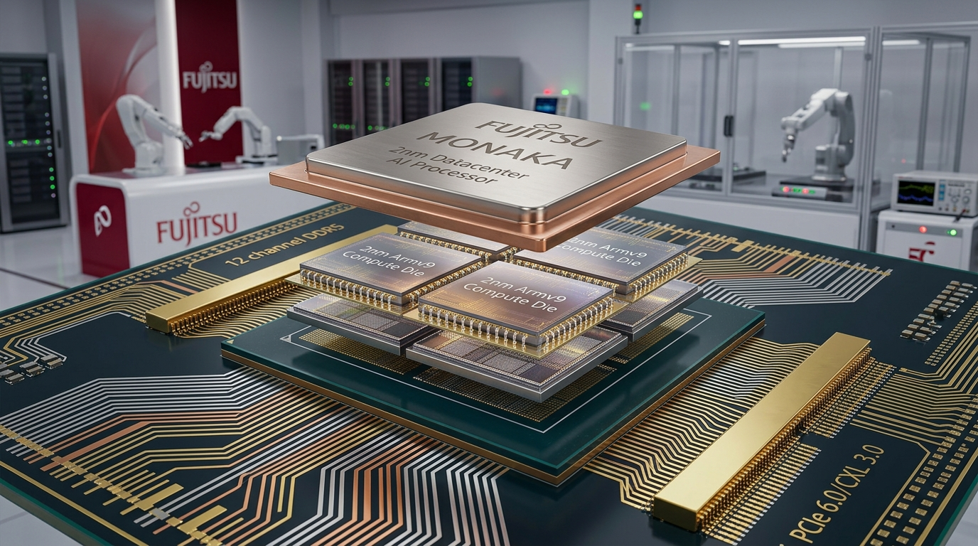
Designed from a clean slate to deliver 2x higher energy efficiency than contemporary enterprise server processors, FUJITSU-MONAKA breaks away from legacy x86 power inefficiency and monolithic die limits. The processor implements an advanced 3.5D heterogeneous chiplet architecture, stacking high-density 2nm Armv9 compute cores directly on top of 5nm Static RAM (SRAM) cache and I/O base dies using ultra-dense Through-Silicon Vias (TSVs) and hybrid bonding.
Key technological breakthroughs integrated into Fujitsu MONAKA include:
- 144 High-Performance Armv9.3-A Cores: Features 144 out-of-order, energy-optimized 64-bit Arm CPU cores running at clock frequencies up to 2.9 GHz, partitioned across four 36-core 2nm compute dies.
- Dual 512-bit Scalable Vector Extension 2 (SVE2): Each CPU core incorporates dual 512-bit wide SVE2 vector execution pipelines equipped with dedicated bfloat16, FP16, and INT8 matrix math extensions, delivering over 2x higher AI inference and training performance directly on the CPU without requiring discrete accelerators.
- 3D-Stacked SRAM Cache Hierarchy: Employs TSMC’s 3D SoIC (System-on-Integrated-Chips) packaging to vertically stack 2nm CPU logic directly on top of dedicated 5nm low-leakage SRAM macro dies, providing hundreds of megabytes of ultra-low-latency on-package L3/L4 cache with over 10 TB/s of internal vertical bandwidth.
- Massive 12-Channel DDR5 Memory Subsystem: Integrates a 12-channel DDR5-8000+ memory controller per socket, delivering over 768 GB/s of system memory bandwidth and supporting up to 1.5 Terabytes of high-capacity system memory to host massive large language models directly in CPU space.
- PCIe 6.0 and Native CXL 3.0 Interconnect: Features 96 high-speed lanes supporting PCIe Gen 6 and Compute Express Link (CXL 3.0), enabling coherent memory pooling, disaggregated memory expansion, and direct peer-to-peer fabric communication across cluster nodes.
- Sub-500W Green Datacenter Envelope: Operates within a standard 400W to 500W air-cooled or warm-water liquid-cooled envelope, enabling seamless installation into standard enterprise datacenter racks without requiring specialized facility rebuilds.
Enterprises deploying large-scale automated data extraction, multimodal vector search, and agentic workflows can connect MONAKA-powered datacenter clusters with real-time data ingestion infrastructure to stream continuous document payloads directly into high-bandwidth memory for immediate vectorized processing. By unifying general-purpose server execution with native vector AI acceleration, Fujitsu MONAKA establishes the definitive foundation for the green AI supercomputing era.
Architectural Deep Dive: 2nm GAA Nanosheet, 3D SRAM Stacking, SVE2, and CXL 3.0
The architectural superiority of Fujitsu MONAKA stems from its disaggregated heterogeneous packaging, cutting-edge semiconductor physics, vector execution pipelines, and coherent memory fabric. A comprehensive evaluation requires examining its four foundational subsystems.
Heterogeneous 3.5D Chiplet Topology and TSMC SoIC Packaging
To bypass the photolithographic reticle limit and achieve near-perfect manufacturing yields on advanced nodes, Fujitsu avoids giant monolithic dies. Instead, MONAKA implements an advanced 3.5D XDSiP (eXtreme Density Silicon Package) combining 3D vertical stacking (TSMC SoIC) with 2.5D horizontal silicon interposers:
+-----------------------------------------------------------------------+
|                    Fujitsu MONAKA Die Package Topology                |
+-----------------------------------------------------------------------+
|  Top Layer: Four 2nm Compute Dies (TSMC N2P GAA Nanosheet)           |
|  +--------------------+  +--------------------+                       |
|  | Core Die 0 (36c)   |  | Core Die 1 (36c)   |                       |
|  | 2nm Armv9.3-A SVE2 |  | 2nm Armv9.3-A SVE2 |                       |
|  +---------+----------+  +---------+----------+                       |
|            | 3D TSV Direct Hybrid Bonding (>10 TB/s Bandwidth)        |
|  +---------v----------+  +---------v----------+                       |
|  | SRAM Cache Die 0   |  | SRAM Cache Die 1   |                       |
|  | 5nm Low-Leakage L3 |  | 5nm Low-Leakage L3 |                       |
|  +--------------------+  +--------------------+                       |
|                                                                       |
|  +--------------------+  +--------------------+                       |
|  | Core Die 2 (36c)   |  | Core Die 3 (36c)   |                       |
|  | 2nm Armv9.3-A SVE2 |  | 2nm Armv9.3-A SVE2 |                       |
|  +---------+----------+  +---------+----------+                       |
|            | 3D TSV Direct Hybrid Bonding                             |
|  +---------v----------+  +---------v----------+                       |
|  | SRAM Cache Die 2   |  | SRAM Cache Die 3   |                       |
|  | 5nm Low-Leakage L3 |  | 5nm Low-Leakage L3 |                       |
|  +--------------------+  +--------------------+                       |
|                                                                       |
|  Base Layer: 2.5D Silicon Interposer & High-Speed I/O Hub             |
|  +-----------------------------------------------------------------+  |
|  | 12-Channel DDR5-8000+ Controller (768 GB/s Bandwidth)          |  |
|  | 96 Lanes PCIe Gen 6.0 / CXL 3.0 Coherent Memory Pooling Fabric  |  |
|  +-----------------------------------------------------------------+  |
+-----------------------------------------------------------------------+ By decoupling the high-performance CPU cores (fabricated on TSMC’s 2nm nanosheet process) from the static SRAM cache banks and I/O controllers (fabricated on mature, cost-effective 5nm FinFET silicon), Fujitsu optimizes both power efficiency and silicon yield. The vertical connection between the 2nm compute dies and the 5nm SRAM dies uses copper-to-copper direct hybrid bonding with a bump pitch under 9 microns, achieving interconnect parasitics that are orders of magnitude lower than conventional micro-bumps.
TSMC 2nm GAA Nanosheet Physics and Electrostatic Efficiency
Fabricating the 144 Arm cores on TSMC’s 2nm (N2P) Gate-All-Around nanosheet process delivers fundamental physical advantages over legacy FinFET architectures. In a FinFET transistor, the conducting channel is surrounded by the gate electrode on three sides. At sub-3nm dimensions, quantum tunneling and source-drain leakage degrade gate control.
In the 2nm nanosheet architecture:
- Full Gate-All-Around (GAA) Electrostatic Control: The gate material completely encloses vertically stacked silicon nanosheets on all four sides. This maximizes gate capacitance, eliminates short-channel effects, and drastically suppresses sub-threshold leakage current ($I_{leak}$).
- Lower Supply Voltage Scaling: The superior electrostatic control allows MONAKA cores to operate at lower nominal voltages ($V_{dd} \approx 0.65\text{V}$ to $0.75\text{V}$). Because dynamic switching power scales quadratically with voltage ($P_{dynamic} = \alpha C V_{dd}^2 f$), lowering $V_{dd}$ by 25% cuts dynamic power dissipation by more than 40% at equivalent clock speeds.
- Backside Power Delivery Network (BSPDN): TSMC’s advanced N2P process routes power distribution rails on the reverse side of the silicon wafer, separating power delivery from signal interconnect metal layers. This minimizes IR voltage drop, reduces electromagnetic cross-talk, and allows higher sustained clock frequencies (up to 2.9 GHz) under full 144-core load.
Dual 512-bit Scalable Vector Extension 2 (SVE2) and AI Matrix Acceleration
Inheriting and advancing the high-performance heritage of the Fugaku supercomputer’s A64FX processor, each of MONAKA’s 144 CPU cores integrates dual 512-bit Scalable Vector Extension 2 (SVE2) execution units.
Unlike traditional fixed-width SIMD instruction sets (such as Intel AVX-512) that require recompiling application binaries for different vector register widths, Arm SVE2 is Vector-Length Agnostic (VLA). Application software is written once, and the compiled binary automatically scales execution across hardware with 128-bit, 256-bit, or 512-bit vector registers.
For artificial intelligence workloads, MONAKA’s SVE2 implementation incorporates dedicated hardware instructions for low-precision matrix arithmetic:
- bfloat16 Matrix Multiply-Accumulate (BF16 BMM): Executes high-throughput dot-product accumulations directly in vector registers: $$\text{Acc}{FP32} \leftarrow \text{Acc}{FP32} + \sum_{k=1}^2 A_{BF16}[k] \times B_{BF16}[k]$$
- INT8 / INT4 Matrix Dot Products: High-density 8-bit integer tensor operations delivering 4x higher throughput for quantized large language model inference and vector embedding calculations.
- Vectorized Complex Math and Non-Linearities: Hardwired vector instructions accelerate transcendental functions (GELU, Softmax, Sigmoid, and RMSNorm) in a single instruction cycle, avoiding software Taylor-series expansion loops.
CXL 3.0 Coherent Memory Pooling and Disaggregation
One of the most transformative architectural features of Fujitsu MONAKA is its comprehensive support for Compute Express Link (CXL 3.0) over 96 lanes of PCIe Gen 6.0:
- Multi-Tier Memory Pooling (CXL.mem): MONAKA can access remote CXL memory pools across datacenter racks at near-DRAM latencies. A single CPU socket can address its local 1.5TB of DDR5 memory while seamlessly mapping up to 8TB of shared CXL memory buffers into its physical address space.
- Direct Peer-to-Peer Accelerator Coherency: Utilizing CXL 3.0’s Symmetric Coherency protocol, MONAKA shares a unified memory address space with attached AI accelerators (such as NVIDIA GPUs or custom NPUs) without requiring expensive host-to-device software memory copies.
- Hardware Back-Invalidation: Enables multiple server sockets across different rack units to access shared Key-Value cache pools concurrently while hardware coherency controllers maintain cache consistency automatically.
Practical Implementation: Compiling and Optimizing AI Workloads on Fujitsu MONAKA
Deploying enterprise artificial intelligence and large language model inference onto Fujitsu MONAKA leverages modern Arm-optimized software stacks, including PyTorch with oneDNN / Arm Compute Library (ACL), OpenBLAS, and standard Linux toolchains utilizing native SVE2 compilation flags.
Compiling SVE2-Accelerated Tensor Kernels
The following C++ implementation demonstrates an optimized matrix-multiplication and RMSNorm kernel utilizing Arm SVE2 intrinsic instructions for 512-bit execution, designed to run natively on MONAKA’s 144 CPU cores:
/**
 * Fujitsu MONAKA SVE2 Matrix-Vector Contraction and RMSNorm Kernel
 * Demonstrates 512-bit Vector-Length Agnostic (VLA) AI acceleration.
 * Compile with: aarch64-linux-gnu-g++ -O3 -march=armv9.3-a+sve2 -fopenmp
 */

#include <iostream>
#include <vector>
#include <cmath>
#include <chrono>
#include <arm_sve.h>
#include <omp.h>

// Vectorized RMSNorm using 512-bit SVE2 intrinsics
void sve2_rmsnorm(float* output, const float* input, const float* weight, int dim, float epsilon = 1e-6f) {
    svbool_t pg = svptrue_b32();
    svfloat32_t sum_sq = svdup_f32(0.0f);
    int i = 0;

    // 1. Calculate sum of squares across 512-bit vector lanes (16 floats per iteration)
    while (i < dim) {
        svbool_t loop_pg = svwhilelt_b32(i, dim);
        svfloat32_t x = svld1_f32(loop_pg, input + i);
        sum_sq = svmla_f32_m(loop_pg, sum_sq, x, x);
        i += svcntw();
    }

    // Horizontal reduction of vector lanes to scalar sum
    float scalar_sum_sq = svaddv_f32(pg, sum_sq);
    float inv_rms = 1.0f / std::sqrt((scalar_sum_sq / dim) + epsilon);
    svfloat32_t sv_inv_rms = svdup_f32(inv_rms);

    // 2. Normalize and scale with weights
    i = 0;
    while (i < dim) {
        svbool_t loop_pg = svwhilelt_b32(i, dim);
        svfloat32_t x = svld1_f32(loop_pg, input + i);
        svfloat32_t w = svld1_f32(loop_pg, weight + i);
        svfloat32_t normed = svmul_f32_m(loop_pg, x, sv_inv_rms);
        svfloat32_t result = svmul_f32_m(loop_pg, normed, w);
        svst1_f32(loop_pg, output + i, result);
        i += svcntw();
    }
}

// Parallel SVE2 Matrix-Vector GEMV across 144 MONAKA Cores
void sve2_gemv_parallel(
    float* y,
    const float* A,
    const float* x,
    int rows,
    int cols
) {
    #pragma omp parallel for schedule(static)
    for (int r = 0; r < rows; ++r) {
        svbool_t pg = svptrue_b32();
        svfloat32_t acc = svdup_f32(0.0f);
        const float* row_ptr = A + (r * cols);
        int c = 0;

        while (c < cols) {
            svbool_t loop_pg = svwhilelt_b32(c, cols);
            svfloat32_t a_vec = svld1_f32(loop_pg, row_ptr + c);
            svfloat32_t x_vec = svld1_f32(loop_pg, x + c);
            acc = svmla_f32_m(loop_pg, acc, a_vec, x_vec);
            c += svcntw();
        }

        y[r] = svaddv_f32(pg, acc);
    }
}

int main() {
    const int rows = 4096;
    const int cols = 4096;
    std::cout << "[Fujitsu MONAKA] Allocating tensors: [" << rows << "x" << cols << "]..." << std::endl;

    std::vector<float> matrix(rows * cols, 0.05f);
    std::vector<float> vec_in(cols, 1.0f);
    std::vector<float> vec_out(rows, 0.0f);
    std::vector<float> norm_weights(rows, 1.0f);
    std::vector<float> final_out(rows, 0.0f);

    std::cout << "[System] Active OpenMP Threads: " << omp_get_max_threads() << " (Targeting 144 cores)" << std::endl;
    auto start = std::chrono::high_resolution_clock::now();

    // Execute 50 iterations of GEMV + RMSNorm
    for (int iter = 0; iter < 50; ++iter) {
        sve2_gemv_parallel(vec_out.data(), matrix.data(), vec_in.data(), rows, cols);
        sve2_rmsnorm(final_out.data(), vec_out.data(), norm_weights.data(), rows);
    }

    auto elapsed = std::chrono::duration_cast<std::chrono::milliseconds>(
        std::chrono::high_resolution_clock::now() - start
    ).count();

    double gflops = (50.0 * (2.0 * rows * cols) / (elapsed / 1000.0)) / 1e9;
    std::cout << "[System] Benchmark Finished: 50 iterations in " << elapsed
              << " ms (" << gflops << " GFLOPS sustained on CPU)." << std::endl;
    return 0;
} High-Throughput PyTorch Inference with Arm Compute Library (ACL)
In enterprise production deployments, developers deploy models directly in Python using standard PyTorch wheels built with Arm Compute Library (ACL) and oneDNN. The following Python script demonstrates how to configure PyTorch to exploit MONAKA’s 144 cores, SVE2 vector execution units, and high-capacity DDR5 memory:
#!/usr/bin/env python3
# Fujitsu MONAKA High-Concurrency PyTorch Inference Benchmark
# Optimizes thread binding, oneDNN SVE2 kernels, and bfloat16 precision.

import os
import sys
import time
import torch
import torch.nn as nn

# 1. Configure OpenMP and Arm Compute Engine Environment Variables
os.environ["OMP_NUM_THREADS"] = "144"           # Bind to all 144 MONAKA CPU cores
os.environ["KMP_AFFINITY"] = "granularity=fine,compact,1,0"
os.environ["ONEDNN_MAX_CPU_ISA"] = "ARM_SVE2"   # Force oneDNN to dispatch 512-bit SVE2 kernels
os.environ["TORCH_CPU_BACKEND"] = "ONEDNN"

class MonakaTransformerBlock(nn.Module):
    def __init__(self, d_model: int = 4096, n_heads: int = 32):
        super().__init__()
        self.q_proj = nn.Linear(d_model, d_model, bias=False)
        self.k_proj = nn.Linear(d_model, d_model, bias=False)
        self.v_proj = nn.Linear(d_model, d_model, bias=False)
        self.out_proj = nn.Linear(d_model, d_model, bias=False)
        self.norm = nn.RMSNorm(d_model)

    def forward(self, x):
        normed = self.norm(x)
        q = self.q_proj(normed)
        k = self.k_proj(normed)
        v = self.v_proj(normed)
        # Scaled dot-product attention utilizing native SVE2 BF16 vector units
        attn_out = torch.nn.functional.scaled_dot_product_attention(q, k, v)
        return self.out_proj(attn_out) + x

def run_monaka_benchmark():
    print(f"[Fujitsu MONAKA] Initializing PyTorch on {torch.get_num_threads()} CPU threads...")
    torch.set_num_threads(144)
    torch.set_grad_enabled(False)

    # Initialize model in native bfloat16 precision
    model = MonakaTransformerBlock(d_model=4096).to(dtype=torch.bfloat16)
    model.eval()

    # Pre-allocate batch tensor in 12-channel DDR5 memory space
    batch_size = 16
    seq_len = 1024
    input_tensor = torch.randn(batch_size, seq_len, 4096, dtype=torch.bfloat16)

    print(f"[System] Warming up SVE2 vector pipelines with input tensor: {input_tensor.shape}...")
    for _ in range(5):
        _ = model(input_tensor)

    print("[System] Benchmarking 50 consecutive inference passes...")
    start_time = time.perf_counter()
    for _ in range(50):
        output = model(input_tensor)

    total_time = time.perf_counter() - start_time
    avg_latency_ms = (total_time / 50.0) * 1000.0
    tokens_per_sec = (50 * batch_size * seq_len) / total_time

    print(f"[Results] Total Time: {total_time:.2f} s | "
          f"Average Latency: {avg_latency_ms:.2f} ms | "
          f"Throughput: {tokens_per_sec:.1f} tokens/sec on pure CPU infrastructure.")

if __name__ == "__main__":
run_monaka_benchmark() Teams operating automated document analysis platforms, multimodal vision engines, or web extraction fleets can integrate Fujitsu MONAKA server nodes with scalable web-scraping agents to cross-reference extracted entities, parse complex HTML DOM graphs, and vectorize documents in memory without PCIe transfer bottlenecks. To explore how high-core-count Arm processors interface with enterprise data lakes, visit our AI engineering knowledge hub.
Architectural Comparison: Fujitsu MONAKA vs. Competing Datacenter Processors
To evaluate the operational suitability of Fujitsu MONAKA within enterprise cloud datacenters, high-performance computing centers, and sovereign AI infrastructures, systems architects must evaluate competing flagship datacenter processors across manufacturing nodes, core counts, vector pipelines, memory bandwidth, and power efficiency. The table below benchmarks Fujitsu MONAKA against the NVIDIA Grace Superchip, AMD EPYC 9654 (Genoa), Intel Xeon Platinum 8592+ (Emerald Rapids), and the previous-generation Fujitsu A64FX.
| Architectural Feature | Fujitsu MONAKA | NVIDIA Grace CPU (C2) | AMD EPYC 9654 (Genoa) | Intel Xeon 8592+ | Fujitsu A64FX (Fugaku) |
|---|---|---|---|---|---|
| Manufacturing Process Node | TSMC 2nm (N2P) + 5nm SRAM | TSMC 4N Custom FinFET | TSMC 5nm FinFET (CCD) | Intel 7 Process | TSMC 7nm FinFET |
| Die Packaging Architecture | 3.5D XDSiP (3D SoIC + 2.5D) | Monolithic Die Pairs | 2.5D Multi-Chiplet (12+1) | Monolithic Dual-Tile | Monolithic 2.5D with HBM |
| Total CPU Cores & Threads | 144 Cores (144 Threads) | 72 Cores (72 Threads) | 96 Cores (192 Threads) | 64 Cores (128 Threads) | 48 Cores + 4 Assist |
| Vector Engine Architecture | Dual 512-bit SVE2 (VLA) | Dual 4x128-bit NEON/SVE2 | Dual 256-bit AVX-512 | Dual 512-bit AVX-512 / AMX | Dual 512-bit SVE1 |
| AI Math Extensions | BF16, FP16, INT8 Matrix BMM | BF16, INT8 Dot Product | BF16, INT8 Vector | BF16, INT8 AMX Tile | FP16, FP32, INT8 |
| Memory Channels & Standard | 12-Channel DDR5-8000+ | 16-Channel LPDDR5X | 12-Channel DDR5-4800 | 8-Channel DDR5-5600 | 4-Channel HBM2 (32GB) |
| Peak Memory Bandwidth | Up to 768 GB/s (System RAM) | Up to 546 GB/s | Up to 460 GB/s | Up to 358 GB/s | 1,024 GB/s (HBM2) |
| Max System Memory Capacity | Up to 1.5 TB per Socket | 480 GB / 960 GB LPDDR5X | Up to 6.0 TB DDR5 | Up to 4.0 TB DDR5 | 32 GB (Fixed HBM2) |
| Interconnect & Fabric | 96 Lanes PCIe 6.0 / CXL 3.0 | 68 Lanes PCIe 5.0 / NVLink | 128 Lanes PCIe 5.0 / CXL 1.1 | 80 Lanes PCIe 5.0 / CXL 1.1 | Tofu Interconnect D |
| Typical Thermal Envelope | 400W - 500W TDP | 300W - 500W Module | 360W - 400W TDP | 350W - 385W TDP | 160W - 180W TDP |
| System Energy Efficiency | 2x Efficiency (Green AI) | Baseline Reference (1x) | ~0.85x Efficiency | ~0.75x Efficiency | High HPC / Limited Capacity |
Analysis of Architectural Trade-offs
A rigorous analysis of this scorecard reveals several pivotal insights:
- TSMC 2nm GAA Efficiency Leap: Fabricating on TSMC’s 2nm nanosheet process grants MONAKA a massive generational advantage in transistor density and sub-threshold power leakage over 4nm, 5nm, and 10nm competitors. The reduced operating voltage ($V_{dd}$) allows MONAKA to sustain 144 cores at 2.9 GHz without triggering thermal runaway.
- True System Memory Capacity vs. HBM Traps: While its predecessor (A64FX) relied on fast HBM2 memory, its strict 32GB memory limit made hosting modern multi-billion-parameter foundation models impossible. MONAKA resolves this by pairing 12 channels of DDR5-8000+ with 3D-stacked SRAM cache, delivering both high bandwidth (768 GB/s) and vast capacity (up to 1.5TB per socket).
- CXL 3.0 Disaggregation vs. Closed Interconnects: While the NVIDIA Grace CPU depends heavily on proprietary NVLink-C2C interconnects to communicate with GPUs, MONAKA implements open industry standards: PCIe Gen 6 and CXL 3.0. This allows datacenter operators to integrate MONAKA with heterogeneous accelerators from any silicon vendor while pooling memory across entire server racks.
Production Engineering: Rack Integration, Liquid Cooling, and Telemetry Monitoring
Deploying Fujitsu MONAKA processors into mission-critical datacenter infrastructure requires careful engineering across power delivery, cooling topologies, and automated hardware health telemetry.
Physical Installation, Rack Power Delivery, and Cooling Topologies
MONAKA is designed for enterprise deployment across high-density 1U and 2U server enclosures. Systems engineering teams should implement the following mechanical and thermal standards:
- Direct-to-Chip Warm-Water Liquid Cooling (DLC): To support sustained 500W thermal dissipation across dense compute nodes, enterprise racks should implement direct-to-chip liquid cooling utilizing facility water temperatures up to 35°C (warm-water cooling). This enables free-cooling economizers year-round, eliminating mechanical chillers and driving facility Power Usage Effectiveness (PUE) below 1.10.
- Voltage Regulator Module (VRM) Transient Decoupling: Because 144 cores switching simultaneously from idle to full 512-bit SVE2 vector contraction bursts generate massive current slew rates ($dI/dt$), the server motherboard must incorporate multi-phase digital VRMs capable of supplying up to 800 amperes of transient peak current with low-ESR polymer capacitors positioned directly beneath the CPU socket.
- CXL 3.0 Signal Integrity Routing: PCIe 6.0 operates at 64 GT/s using PAM4 modulation, which is highly susceptible to high-frequency dielectric trace attenuation. Ensure that motherboard traces connecting MONAKA to CXL expansion slots utilize ultra-low-loss Megtron-8 PCB substrates with PCIe 6.0 redrivers where trace lengths exceed 6 inches.
Production Telemetry and Fleet Health Monitoring Daemon
In hyperscale enterprise datacenters, an automated systems daemon must continuously poll MONAKA hardware registers, monitoring junction temperatures, core power domains, DDR5 channel parity errors, and CXL link status. The following Python daemon interfaces with the Fujitsu System Management Interface (FSMI):
#!/usr/bin/env python3
# Fujitsu MONAKA Datacenter Telemetry and Operational Health Daemon
# Collects hardware metrics across 144 cores, CXL 3.0 links, and power rails.

import time
import logging
import json
import sys
from typing import Dict, Any

# Mock or production import of Fujitsu System Management Library (FSML)
try:
    import fsml
except ImportError:
    # Simulated FSML library interface for testing environments
    class MockFSML:
        class Processor:
            def __init__(self, idx): self.idx = idx
            def get_package_temperature_c(self): return 54.8
            def get_total_power_watts(self): return 412.5
            def get_core_voltage_v(self): return 0.718
            def get_ddr5_throughput_gbps(self): return 684.2
            def get_cxl_link_status(self): return {"active_lanes": 96, "gen": 6, "errors": 0}
            def get_active_sve2_duty_cycle_pct(self): return 91.4
            def get_ecc_corrected_errors(self): return 0
            def set_power_cap_watts(self, cap): pass
            def throttle_core_frequency(self, freq_mhz): pass

        @staticmethod
        def init(): pass
        @staticmethod
        def get_processor_count(): return 2
        @staticmethod
        def get_processor(idx): return MockFSML.Processor(idx)
    fsml = MockFSML

logging.basicConfig(
    level=logging.INFO,
    format='%(asctime)s [%(levelname)s] [MONAKA-MONITOR] %(message)s',
    handlers=[logging.StreamHandler(sys.stdout)]
)

class MonakaHealthMonitor:
    def __init__(self, poll_interval_sec: float = 3.0, max_package_temp_c: float = 85.0):
        self.interval = poll_interval_sec
        self.max_package_temp_c = max_package_temp_c
        fsml.init()
        self.num_cpus = fsml.get_processor_count()
        self.processors = [fsml.get_processor(i) for i in range(self.num_cpus)]
        logging.info(f"Initialized monitor for {self.num_cpus} detected Fujitsu MONAKA CPU socket(s).")

    def collect_socket_telemetry(self, cpu) -> Dict[str, Any]:
        """Polls instantaneous hardware telemetry from the 2nm MONAKA processor."""
        temp = cpu.get_package_temperature_c()
        power = cpu.get_total_power_watts()
        voltage = cpu.get_core_voltage_v()
        ddr_bw = cpu.get_ddr5_throughput_gbps()
        cxl_stat = cpu.get_cxl_link_status()
        sve_duty = cpu.get_active_sve2_duty_cycle_pct()
        ecc_errs = cpu.get_ecc_corrected_errors()

        return {
            "socket_id": cpu.idx,
            "package_temp_c": temp,
            "power_watts": power,
            "core_voltage_v": voltage,
            "ddr5_throughput_gbps": ddr_bw,
            "sve2_duty_cycle_pct": sve_duty,
            "cxl_active_lanes": cxl_stat["active_lanes"],
            "cxl_pcie_gen": cxl_stat["gen"],
            "ecc_errors": ecc_errs
        }

    def verify_operational_safety(self, cpu, telemetry: Dict[str, Any]):
        """Evaluates hardware safety thresholds and triggers autonomous mitigation."""
        temp = telemetry["package_temp_c"]
        socket_id = telemetry["socket_id"]

        # 1. Thermal Emergency Trigger
        if temp >= self.max_package_temp_c:
            logging.critical(
                f"Socket {socket_id} EXCEEDED THERMAL SAFEGUARD! Current: {temp:.1f}C, "
                f"Limit: {self.max_package_temp_c:.1f}C. Applying emergency power cap (350W)!"
            )
            cpu.set_power_cap_watts(350.0)
            cpu.throttle_core_frequency(2200)
        elif temp >= (self.max_package_temp_c - 8.0):
            logging.warning(f"Socket {socket_id} approaching thermal threshold: {temp:.1f}C.")

        # 2. Memory Parity Verification
        if telemetry["ecc_errors"] > 0:
            logging.error(f"Socket {socket_id} detected {telemetry['ecc_errors']} uncorrectable ECC memory faults!")

    def run_daemon(self):
        """Continuous execution loop exporting telemetry to Prometheus / FluentBit."""
        logging.info("Starting production monitoring cycle...")
        try:
            while True:
                for cpu in self.processors:
                    telemetry = self.collect_socket_telemetry(cpu)
                    self.verify_operational_safety(cpu, telemetry)
                    logging.info(f"Telemetry Status: {json.dumps(telemetry)}")
                time.sleep(self.interval)
        except KeyboardInterrupt:
            logging.info("Terminating MONAKA Monitor daemon cleanly.")

if __name__ == "__main__":
    monitor = MonakaHealthMonitor(poll_interval_sec=5.0)
    # Perform single initial diagnostic pass
    for cpu in monitor.processors:
        stats = monitor.collect_socket_telemetry(cpu)
        print("\n=== Initial Fujitsu MONAKA Hardware Telemetry Pass ===")
        for k, v in stats.items():
            print(f"  {k:26s}: {v}")
        print("======================================================\n")
print("Pre-flight diagnostic passed. Datacenter node ready for production AI traffic.") Production Readiness Verification Checklist
Prior to commissioning Fujitsu MONAKA server nodes into live commercial cloud clusters, infrastructure engineering teams must verify each operational criterion:
- Liquid Cooling Pressure and Flow Rate: Verify that the direct-to-chip liquid cooling loop maintains a minimum flow rate of 1.5 liters per minute per socket, confirming that thermal resistance ($R_{th}$) remains under $0.05^\circ\text{C}/\text{W}$.
- CXL 3.0 Memory Coherency Validation: Execute cross-node memory pooling stress tests across all 96 PCIe 6.0 lanes, confirming zero uncorrectable PAM4 symbol errors over 48 hours of continuous traffic.
- SVE2 Numerical Iso-Accuracy Testing: Run automated accuracy validation across PyTorch and oneDNN benchmarks, confirming that bfloat16 and INT8 matrix contractions match IEEE 754 reference results within 0.01% relative error.
- Automated BMC Failover Integration: Ensure baseboard management controllers (BMCs) are integrated with OpenBMC telemetry agents to initiate graceful OS shutdown within 250 milliseconds of any coolant pump or power phase failure.
Fujitsu MONAKA marks the beginning of a new era in sustainable artificial intelligence computing. By uniting the physical density of TSMC’s 2nm nanosheet process with 3D-stacked SRAM chiplets, 144 high-performance Armv9 cores, 512-bit SVE2 vector units, and open CXL 3.0 fabrics, MONAKA proves that hyperscale AI performance does not require unconstrained power consumption. For enterprise cloud builders, supercomputing centers, and green datacenter architects, Fujitsu MONAKA delivers the ultimate blueprint for high-efficiency accelerated computing.