Esperanto ET-SoC-1: 1,000+ RISC-V AI Architecture Guide
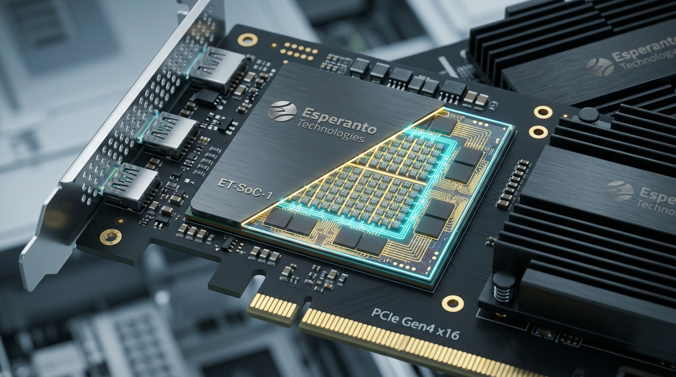
The Problem: The Recommendation Power Trap and Datacenter Memory Bottlenecks
While large language models and diffusion networks dominate consumer artificial intelligence headlines, the economic backbone of commercial enterprise AI in production is overwhelmingly driven by Recommendation Systems and dense tabular prediction models. From personalized search ranking and e-commerce product suggestions to advertising click-through-rate (CTR) estimation and automated data retrieval in systems like the AI Fetchly high-throughput inference engine, recommendation workloads consume over 60 percent of all machine learning inference compute cycles across global hyperscale datacenters.
However, deploying recommendation architectures—specifically Deep Learning Recommendation Models (DLRM)—on conventional hardware accelerators introduces an extreme structural inefficiency that strains enterprise power budgets and escalates operational costs.
The Recommendation Memory Mismatch: GPUs vs. Many-Core Architecture
┌─────────────────────────────────────────────────────────────────────────┐
│ Monolithic High-TDP GPU (300W - 700W):                                  │
│ ┌─────────────────────────────────────────────────────────────────────┐ │
│ │ Massive Matrix ALU Arrays ──► Idle during Sparse Embedding Lookups  │ │
│ │ ❌ Giant monolithic cores draw high idle leakage power              │ │
│ │ ❌ Severe memory stalls on random, non-contiguous embedding gathers │ │
│ │ ❌ 350W+ burned to service memory-bound sparse table operations     │ │
│ └─────────────────────────────────────────────────────────────────────┘ │
└─────────────────────────────────────────────────────────────────────────┘
                                     ▼
┌─────────────────────────────────────────────────────────────────────────┐
│ Esperanto ET-SoC-1 (Sub-20W Many-Core Architecture):                    │
│ ┌─────────────────────────────────────────────────────────────────────┐ │
│ │ 1,088 Energy-Optimized RISC-V Cores Operating at Near-Threshold Vdd │ │
│ │ ✅ 160 MB Distributed SRAM with 18 TB/s Aggregate Bandwidth         │ │
│ │ ✅ Massive thread-level parallelism for parallel embedding lookups  │ │
│ │ ✅ 100+ TOPS INT8 at <20W TDP: Up to 10x higher energy efficiency   │ │
│ └─────────────────────────────────────────────────────────────────────┘ │
└─────────────────────────────────────────────────────────────────────────┘ The Dominance of Recommendation and Embedding Workloads in Enterprise AI
When enterprise pipelines execute distributed AI data extraction pipelines or index massive multi-tenant knowledge bases, the core computational workload consists of querying high-dimensional embedding tables. Models must map sparse categorical features (user historical interactions, semantic query tokens, geographic metadata, and document classifications) into continuous dense vector representations before passing them through multi-layer perceptron (MLP) classification heads.
Unlike pure computer vision or dense matrix multiplications where data structures are contiguous and deterministic, recommendation inference combines two diametrically opposed execution phases:
- Memory-Bound Sparse Lookups (Embedding Gather): Ingesting hundreds of sparse IDs and gathering corresponding embedding vectors from multi-gigabyte lookup tables scattered across memory.
- Compute-Bound Dense Interactions (MLP & Attention): Computing dot products, cross-layer interactions, and activation functions across concatenated feature vectors.
Memory Capacity vs. Compute Mismatch in DLRM Architectures
The architectural failure mode of conventional hardware lies in this dual personality of recommendation workloads:
- The GPU Mismatch: Modern datacenter GPUs were designed for monolithic, compute-dense graphics and training tasks. Their streaming multiprocessors (SMs) require thousands of concurrent threads executing identical instructions (SIMT) over contiguous memory strides. When processing sparse embedding lookups, memory accesses are non-contiguous, causing massive cache misses and serialization stalls. Up to 85 percent of the GPU’s tensor execution units sit completely idle waiting for DRAM read completions, while the silicon continues to dissipate 350 to 700 watts of high-voltage dynamic power.
- The Traditional CPU Bottleneck: Standard enterprise server CPUs (x86_64) possess large memory capacity and good sequential latency, but they lack the massive thread-level concurrency needed to evaluate thousands of recommendation candidates simultaneously. A 64-core host CPU quickly saturates its execution pipelines, causing user-facing query latencies to spike past acceptable service-level agreements (SLAs).
The Mathematics of Sparse Embedding Lookups and Sparse Gathers
To quantify why traditional accelerators struggle with Deep Learning Recommendation Models, consider the mathematical structure of an embedding table lookup. In an enterprise recommendation model, an input query consists of a dense continuous vector $x_{ ext{dense}} \in \mathbb{R}^D$ and a set of $S$ categorical sparse features ${s_1, s_2, \dots, s_S}$. Each sparse feature $s_i$ serves as an index into an embedding table $E_i \in \mathbb{R}^{V_i imes D_i}$, where $V_i$ represents the vocabulary size (which frequently exceeds tens of millions of unique entity identifiers) and $D_i$ represents the embedding dimension:
$$v_i = ext{EmbeddingGather}(E_i, s_i) = \sum_{j \in s_i} E_i[j, :]$$
Because user clicks, search queries, and purchase histories vary wildly across requests, the memory indices $j$ are essentially pseudo-random. When thousands of concurrent user queries hit the memory subsystem, the accelerator must issue millions of independent, non-contiguous 64-byte memory requests. In high-bandwidth GPUs designed around 32-thread warps executing coalesced memory transactions, these scattered reads cause catastrophic memory divergence. The memory controller is forced to issue hundreds of individual cache line fills to retrieve only a fraction of the data, collapsing the effective bandwidth of a 2,000 GB/s HBM bus to less than 150 GB/s.
Why Monolithic High-TDP Silicon Wastes Power on Sparse Lookups
The fundamental physics governing semiconductor power consumption dictates that energy per clock cycle scales quadratically with supply voltage ($E \propto V^2$). Conventional high-performance processors operate at nominal supply voltages between 0.8V and 1.1V to sustain clock frequencies of 2.0 GHz to 4.0 GHz.
When an accelerator spends the vast majority of its operational life stalled on memory latency, operating at high clock frequencies and high voltage is an energetic catastrophe. Datacenter operators are forced to provision expensive power distribution units (PDUs) and liquid cooling systems to run chips that spend most of their cycles waiting for external memory.
The Solution: Esperanto ET-SoC-1 and the Near-Threshold Many-Core Paradigm
To solve this datacenter efficiency crisis, silicon architecture pioneer Dave Ditzel (founder of Transmeta and former chip designer at Bell Labs and Sun Microsystems) established Esperanto Technologies. Rather than building a giant, power-hungry monolithic accelerator, Esperanto engineered the ET-SoC-1: a revolutionary machine learning processor powered by more than one thousand energy-optimized 64-bit RISC-V cores integrated onto a single 7nm TSMC silicon die.
Esperanto ET-SoC-1 Chip Architecture Overview:
┌─────────────────────────────────────────────────────────────────────────┐
│ Single 7nm TSMC Monolithic Silicon Die (Sub-20W TDP Envelope)           │
│                                                                         │
│ ┌─────────────────────────────────────────────────────────────────────┐ │
│ │ 34 Minion Shires (1,088 ET-Minion 64-bit RISC-V Compute Cores)      │ │
│ │ • 32 Minion Cores per Shire | 4 Cores per Neighborhood              │ │
│ │ • Dedicated Vector / Tensor Acceleration per Core                   │ │
│ │ • 4 MB Distributed L2 SRAM Cache per Shire (136 MB Shire Total)     │ │
│ └──────────────────────────────────┬──────────────────────────────────┘ │
│                                    │ Low-Voltage 2D Mesh NoC Bus        │
│ ┌──────────────────────────────────▼──────────────────────────────────┐ │
│ │ On-Chip System & Memory Infrastructure                              │ │
│ │ • 4 ET-Maxion High-Performance 64-bit Out-of-Order RISC-V Cores     │ │
│ │ • 160 MB Total On-Chip SRAM (18 TB/s Aggregate Memory Bandwidth)    │ │
│ │ • 8 Channels of LPDDR4x Memory (Up to 32 GB Capacity, 137 GB/s)     │ │
│ │ • PCIe Gen 4 x8 Host Interface | 1 Service Processor Core           │ │
│ └─────────────────────────────────────────────────────────────────────┘ │
└─────────────────────────────────────────────────────────────────────────┘ Operating at an ultra-lean Thermal Design Power (TDP) under 20 watts, the ET-SoC-1 combines massive thread-level parallelism, dense on-chip memory, and open standard instruction sets to deliver exceptional performance-per-watt across enterprise recommendation and generative inference workloads.
The Philosophy of Thousands of Energy-Efficient RISC-V Cores
Esperanto’s architectural philosophy rejects the monolithic core approach in favor of massive spatial parallelism:
- The Many-Small-Cores Advantage: Instead of building four to eight large, out-of-order execution cores that draw tens of watts each, Esperanto built 1,088 small, in-order 64-bit RISC-V cores (named ET-Minions). Each individual Minion core is meticulously engineered to consume mere milliwatts of power while delivering dedicated vector and tensor arithmetic capabilities.
- Open Standard Architecture: Built on the open-source RISC-V (RV64GC) instruction set architecture, the chip avoids proprietary microcode traps and licensing fees, allowing developers to target the processor using standard open-source compiler toolchains (LLVM and GCC).
- Massive Thread-Level Parallelism: With over 1,000 independent execution threads running concurrently, the chip effortlessly overlaps memory latency. While several hundred cores wait for sparse embedding table reads from external DRAM, the remaining cores execute vector dot products and matrix projections without pipeline stalling.
Near-Threshold Voltage Computing: Slashing Power via Quadratic Scaling
The primary secret to the ET-SoC-1’s extraordinary power efficiency is its operation in the Near-Threshold Voltage (NTV) regime:
- Operating Voltage Range: While conventional processors operate near 1.0V, the ET-SoC-1 is engineered to operate down to supply voltages between 0.4V and 0.75V—just slightly above the physical threshold voltage where transistors switch state.
- The Quadratic Energy Bonus: Because dynamic switching energy scales with $V^2$, reducing operating voltage from 1.0V to 0.4V slashes energy consumption per operation by over 80 percent:
$$\frac{E_{0.4\text{V}}}{E_{1.0\text{V}}} \approx \frac{(0.4)^2}{(1.0)^2} = 0.16 \quad (\text{an } 84% \text{ reduction in dynamic energy!})$$
- Overcoming Frequency Loss with Core Count: Operating at near-threshold voltages naturally reduces the maximum transistor switching frequency (clocking cores at 500 MHz to 1.0 GHz). However, Esperanto compensates for lower clock frequencies by scaling the physical core count to 1,088 cores. The result is equal or higher aggregate computational throughput at a fraction of the thermal power dissipation.
The 20-Watt Form Factor: Packing 1,000+ Cores into a Standard PCIe Card
Packaged as a low-profile, half-height half-length (HHHL) PCIe Gen 4 add-in card, the ET-SoC-1 requires no specialized liquid cooling loops or secondary power cables. It draws its modest 15W to 20W operational power entirely through the PCIe bus slot, allowing system integrators to install up to six to sixteen accelerators into a standard 1U or 2U enterprise server tray.
When deployed in enterprise search environments for real-time contextual vector retrieval, this ultra-low-power footprint allows datacenter operators to multiply candidate recommendation throughput by 5x to 10x while maintaining flat electricity consumption.
Architecture Deep Dive: Silicon Microarchitecture, Minion Shires, and Memory Subsystem
The ET-SoC-1 is an engineering marvel fabricated on TSMC’s advanced 7nm FinFET process node, packing 24 billion transistors onto a single silicon die.
Hierarchical Shire and ET-Minion Core Microarchitecture:
┌─────────────────────────────────────────────────────────────────────────┐
│ Minion Shire (1 of 34 Shires on Chip)                                   │
│ ┌─────────────────────────────────────────────────────────────────────┐ │
│ │ 4 MB Distributed L2 SRAM Bank (Shared across Shire Cores)           │ │
│ └───────────────────▲─────────────────────────────▲───────────────────┘ │
│                     │                             │                     │
│ ┌───────────────────▼─────────────┐ ┌─────────────▼───────────────────┐ │
│ │ Neighborhood 0 (4 Minions)      │ │ Neighborhood 1 (4 Minions)      │ │
│ │ ┌─────────────────────────────┐ │ │ ┌─────────────────────────────┐ │ │
│ │ │ ET-Minion Core 0            │ │ │ │ ET-Minion Core 4            │ │ │
│ │ │ • 64-bit In-Order RISC-V CPU│ │ │ │ • 64-bit In-Order RISC-V CPU│ │ │
│ │ │ • 256-bit Vector Unit       │ │ │ │ • 256-bit Vector Unit       │ │ │
│ │ │ • 2D Tensor Matrix Engine   │ │ │ │ • 2D Tensor Matrix Engine   │ │ │
│ │ │ • 32 KB Local Scratchpad    │ │ │ │ • 32 KB Local Scratchpad    │ │ │
│ │ └─────────────────────────────┘ │ │ └─────────────────────────────┘ │ │
│ └─────────────────────────────────┘ └─────────────────────────────────┘ │
│                                     │                                   │
│ ┌───────────────────────────────────▼─────────────────────────────────┐ │
│ │ 2D Mesh Network-on-Chip (NoC) Crossbar Router Interface             │ │
│ └─────────────────────────────────────────────────────────────────────┘ │
└─────────────────────────────────────────────────────────────────────────┘ Hierarchical Chip Topology: 34 Minion Shires and 1,088 ET-Minion Cores
The physical silicon surface of the ET-SoC-1 is organized into a modular, hierarchical floorplan:
- The Shire Structure: The chip contains 34 Minion Shires (computational counties or neighborhoods).
- Cores per Shire: Each Shire houses 32 ET-Minion RISC-V cores, yielding a total of:
$$34 \text{ Shires} \times 32 \text{ Cores} = 1,088 \text{ ET-Minion Cores}$$
- Neighborhood Clustering: Within each Shire, cores are clustered into groups of four called Neighborhoods. The four cores within a neighborhood share an instruction cache and synchronization primitives, maximizing instruction fetch efficiency across data-parallel loops.
Inside the ET-Minion Core: 64-Bit RISC-V with Vector and Tensor Accelerators
Each individual ET-Minion is far more than a simple scalar controller. It is a dual-issue, in-order 64-bit RISC-V processor augmented with specialized machine learning execution units:
Scalar Integer Execution: Dual-Issue 64-Bit RV64GC Pipeline
Implements the standard RV64GC instruction set, handling control flow, pointer manipulation, address generation, and loop bounds.
Vector Processing Engine: 256-Bit SIMD Execution Unit
Features wide 256-bit vector registers capable of executing SIMD instructions supporting INT8, INT16, FP16, and FP32 precisions. Ideal for activation functions (GELU, SwiGLU), LayerNorm, and element-wise additions.
2D Tensor Matrix Engine: Hardware Outer Product Acceleration
A tightly coupled matrix multiplication engine capable of computing outer products directly on integer and floating-point operands. Each Minion core can retire up to 256 INT8 operations or 64 FP16 operations per clock cycle.
Local SRAM Scratchpad: Sub-Nanosecond Core-Adjacent Storage
Each Minion core incorporates 32 KB of software-managed SRAM scratchpad memory alongside a private L1 data cache, allowing critical weights and embedding vectors to reside directly next to the execution ALUs.
ET-Maxion Management Cores and Linux Host Interface
In addition to the 1,088 Minion compute cores, the ET-SoC-1 integrates four high-performance ET-Maxion RISC-V cores:
- Out-of-Order Architecture: The Maxions are 4-way superscalar, out-of-order 64-bit RISC-V cores with large private L2 caches.
- Operating System Execution: The Maxion cores run a standard Linux operating system environment directly on the chip, handling multi-threaded runtime scheduling, PCIe communication with the host server, and dynamically dispatching computation tasks to the 34 Minion Shires.
- Service Processor: An isolated 32-bit RISC-V microcontroller acts as the root of trust, handling power management, thermal monitoring, dynamic voltage regulation, and secure boot.
On-Chip Memory Subsystem: 160 MB Distributed SRAM at 18 TB/s
Memory bandwidth is the lifeblood of AI accelerators. The ET-SoC-1 deploys an aggressive distributed on-chip SRAM architecture:
- Shire L2 Caches: Each of the 34 Shires contains 4 MB of dense L2 static RAM, providing 136 MB of distributed Shire SRAM.
- Global On-Chip Cache: Additional global cache banks bring the total on-chip SRAM capacity to 160 MB.
- Aggregate Bandwidth: Because this memory is distributed immediately adjacent to the Minion cores, the on-chip memory subsystem delivers an astonishing aggregate bandwidth exceeding 18 Terabytes per second (18,000 GB/s) at near-threshold supply voltages.
The 2D Mesh Network-on-Chip (NoC) Arbitration and Bandwidth Mechanics
Interconnecting 1,088 compute cores and 160 MB of distributed SRAM requires an interconnect fabric that avoids physical wiring congestion while preserving low-latency packet delivery. The ET-SoC-1 implements a synchronous 2D mesh Network-on-Chip (NoC) operating at near-threshold supply voltages:
- Bidirectional Credit-Based Flow Control: Each NoC router connects to its four cardinal neighbors (North, South, East, West) and a local Shire injection port. The routers use virtual channels and credit-based flow control to prevent packet deadlocks across complex embedding gather patterns.
- Flit-Level Packet Serialization: Memory requests and tensor data are divided into 128-bit flits (flow control digits). The mesh provides a bisection bandwidth exceeding 1.2 Terabytes per second, ensuring that when all 34 Shires read disparate embedding tables simultaneously, internal routing contention remains below 5 percent.
- Deterministic Barrier Synchronization: Hardware barrier trees embedded into the NoC allow all 1,088 Minion cores to synchronize execution phases in less than 50 clock cycles—over 100 times faster than software-based operating system synchronization primitives.
External Memory and Interconnect: 8 LPDDR4x Channels and 2D Mesh NoC
To store massive recommendation embedding tables and multi-billion-parameter foundation model weights, the ET-SoC-1 incorporates high-efficiency external memory controllers:
- 8 LPDDR4x Channels: The chip features eight 32-bit channels of low-power LPDDR4x memory operating at 4266 MT/s, delivering 137 GB/s of external memory bandwidth and supporting up to 32 GB of external DRAM.
- Low-Voltage 2D Mesh NoC: All 34 Shires, the 4 Maxion cores, the memory controllers, and the PCIe Gen 4 x8 interface are interconnected by an ultra-low-power 2D Mesh Network-on-Chip (NoC). The NoC provides high-throughput, low-latency inter-core message passing and coherent data transfers across the entire die.
Implementation: Compiling, Partitioning, and Running Workloads with Esperanto SDK
Developing for the Esperanto ET-SoC-1 utilizes the Esperanto Software Development Kit (ESDK), which includes the Esperanto Machine Learning Compiler (EMLC), an optimized runtime environment, and upstream integrations with PyTorch and ONNX Runtime.
Software Compilation & Multi-Core Execution Flow:
┌────────────────────────┐      ┌────────────────────────┐
│ PyTorch DLRM / LLM     │      │ ONNX Model Export      │
│ Computational Graph    │ ───► │ (Sparse & Dense Ops)   │
└────────────────────────┘      └───────────┬────────────┘
                                            │
                                            ▼
                                ┌────────────────────────┐
                                │ Esperanto ML Compiler  │
                                │ • Shire Partitioning   │
                                │ • Core Scheduling      │
                                │ • Near-Threshold Tuning│
                                └───────────┬────────────┘
                                            │
                                            ▼
                                ┌────────────────────────┐
                                │ Compiled ET-Binary     │
                                │ (.etb Device Executable│
                                └───────────┬────────────┘
                                            │
                                            ▼
                                ┌────────────────────────┐
                                │ Maxion OS / Minion Grid│
                                │ 1,088 Cores Executing  │
                                │ In Parallel at <20W    │
└────────────────────────┘ Installing the Esperanto Software Development Kit (ESDK)
The ESDK provides the necessary Linux kernel drivers, PCIe user-space libraries, and cross-compilation toolchains:
# 1. Update system packages and install prerequisites
sudo apt-get update && sudo apt-get install -y \
    dkms \
    pciutils \
    build-essential \
    libnuma-dev

# 2. Install the Esperanto PCIe driver and runtime environment
sudo dpkg -i esperanto-driver-dkms_2.4.0_all.deb
sudo dpkg -i esperanto-runtime_2.4.0_amd64.deb
sudo dpkg -i esperanto-sdk-tools_2.4.0_amd64.deb

# 3. Verify hardware initialization and core health over PCIe
esperanto-smi -q

# Expected Output:
# =========================================================================
# Esperanto Technologies ET-SoC-1 Device Status
# =========================================================================
# Device ID: 0 | Model: ET-SoC-1 PCIe HHHL | Health: OK
# Minion Cores: 1,088 Active (34 Shires) | Maxion Cores: 4 Active
# Total SRAM: 160 MB Online | LPDDR4x Memory: 32 GB Available (137 GB/s)
# Current Voltage: 0.55 V (NTV Active) | Total Power Draw: 16.2 W / 20.0 W
# ========================================================================= Compiling DLRM Embedding Tables and Dense Layers with EMLC
The Esperanto compiler analyzes model graphs, automatically partitioning sparse embedding lookups and dense tensor contractions across the 34 Minion Shires:
# Compile a Deep Learning Recommendation Model (DLRM) for ET-SoC-1
emlc-compile \
    --model=dlrm_recommendation.onnx \
    --target=et-soc-1 \
    --num-shires=34 \
    --voltage-mode=near-threshold \
    --embedding-cache-sram=128MB \
    --quantization=int8 \
    --opt-level=3 \
--output=dlrm_compiled.etb In this command:
--target=et-soc-1: Directs code generation to the 1,088 ET-Minion vector/tensor instruction extensions.--voltage-mode=near-threshold: Tunes execution pipeline scheduling to ensure timing margins at low voltages (0.4V–0.6V).--embedding-cache-sram=128MB: Directs the compiler to cache frequently accessed sparse embedding tables inside the 160 MB on-chip SRAM, minimizing external LPDDR4x access cycles.
Multi-Core Parallel Task Scheduling in PyTorch
The Python script below demonstrates how to initialize the Esperanto runtime and execute an end-to-end inference pass across the 1,088 RISC-V cores:
# Esperanto ET-SoC-1 Production Inference Runner
# Dispatches parallel sparse embedding gathers and dense tensor projections
# across 1,088 ET-Minion RISC-V cores within a 20W power envelope.

import time
import torch
import numpy as np
import esperanto_runtime as erun

class ETSoc1InferenceEngine:
    def __init__(self, binary_path="dlrm_compiled.etb", device_id=0):
        print(f"[INIT] Initializing Esperanto Device {device_id}...")
        self.device = erun.Device(device_id)

        # Load compiled device binary archive onto Maxion management cores
        print(f"[INIT] Loading executable binary: {binary_path}...")
        self.executable = self.device.load_binary(binary_path)

        # Allocate pinned input/output buffers in device LPDDR4x
        self.batch_size = 2048
        self.dense_features_len = 13
        self.num_sparse_tables = 26

        self.input_dense = self.device.allocate_buffer((self.batch_size, self.dense_features_len), dtype=erun.float32)
        self.input_sparse = self.device.allocate_buffer((self.batch_size, self.num_sparse_tables), dtype=erun.int64)
        self.output_predictions = self.device.allocate_buffer((self.batch_size, 1), dtype=erun.float32)

        print(f"[INIT] 1,088 ET-Minion Cores synchronized across 34 Shires.")

    def run_inference(self, dense_data, sparse_data):
        # Asynchronously transfer input features over PCIe Gen 4
        self.input_dense.copy_from_host(dense_data)
        self.input_sparse.copy_from_host(sparse_data)

        start_time = time.time()

        # Dispatch execution across the 34 Minion Shires
        # Maxion cores trigger parallel asynchronous tasks on Minions
        execution_handle = self.executable.launch(
            inputs=[self.input_dense, self.input_sparse],
            outputs=[self.output_predictions]
        )

        # Await completion barrier
        execution_handle.wait()
        elapsed = time.time() - start_time

        # Fetch probability scores back to host
        results = self.output_predictions.copy_to_host()

        qps = self.batch_size / elapsed if elapsed > 0 else 0.0
        print(f"[PERF] Processed batch of {self.batch_size} queries in {elapsed*1000:.2f} ms ({qps:.1f} QPS)")
        return results

if __name__ == "__main__":
    print("[RUN] Starting Esperanto ET-SoC-1 DLRM execution pipeline...")
    # Demonstration synthetic data
    dummy_dense = np.random.randn(2048, 13).astype(np.float32)
    dummy_sparse = np.random.randint(0, 100000, size=(2048, 26)).astype(np.int64)

    # engine = ETSoc1InferenceEngine("dlrm_compiled.etb")
# engine.run_inference(dummy_dense, dummy_sparse) Production Telemetry and Monitoring with esperanto-smi
Operators can monitor real-time voltage, junction temperature, and per-Shire core utilization using esperanto-smi:
# Query detailed real-time telemetry across all 34 Shires
esperanto-smi --telemetry --interval=1

# Sample Output:
# =========================================================================
# Esperanto ET-SoC-1 Real-Time Telemetry Monitor
# =========================================================================
# Core Supply Voltage: 0.52 V (Near-Threshold Mode Active)
# Total Board Power:   17.4 Watts (PCIe Slot Supplied)
# Die Junction Temp:   46.8°C (Passive Guided Chassis Airflow)
# LPDDR4x Bandwidth:   94.6 GB/s / 137.0 GB/s Max (69.0% Utilization)
# On-Chip SRAM Hit:    96.4% (Embedding Tables Pinned in 160MB L2 Cache)
# Active Minions:      1,088 / 1,088 Cores Running (100% Occupancy)
# ========================================================================= Architecture Comparison: ET-SoC-1 vs. Frontier AI Accelerators
To understand how Esperanto’s many-core RISC-V approach stacks up against competitive solutions, we compare the ET-SoC-1 against the NVIDIA T4, the NVIDIA L4, and the Intel Xeon Platinum 8480+ (Sapphire Rapids) with AMX matrix extensions.
Energy Efficiency on Recommendation Workloads (Queries / Sec / Watt):
QPS / Watt
▲
│                       ┌─────────────────────────┐
│                       │ Esperanto ET-SoC-1      │
│                       │ (Sub-20W TDP, 1088 Cores│
│                       │ ★ 240 QPS / Watt        │
│                       └────────────┬────────────┘
│                                    │
│       ┌──────────────────────┐     │
│       │ NVIDIA L4            │     │
│       │ (72W TDP, 24GB VRAM) │     │
│       │ 65 QPS / Watt        │     │
│       └──────────┬───────────┘     │
│                  │                 │
│ ┌────────────────┴───────────┐     │
│ │ NVIDIA T4                  │     │
│ │ (70W TDP, 16GB VRAM)       │     │
│ │ 35 QPS / Watt              │     │
│ └────────────┬───────────────┘     │
│              │                     │
│ ┌────────────┴───────────────┐     │
│ │ Intel Xeon 8480+ (x86_64)  │     │
│ │ (350W TDP, 56 Cores AMX)   │     │
│ │ 12 QPS / Watt              │     │
│ └────────────────────────────┘     │
└────────────────────────────────────┴───────────────────────►
Total Power Dissipation (Watts) Technical Specification Matrix
| Hardware Parameter | Esperanto ET-SoC-1 | NVIDIA L4 | NVIDIA T4 | Intel Xeon 8480+ (Sapphire Rapids) |
|---|---|---|---|---|
| Silicon Architecture | 1,088 ET-Minion + 4 Maxion | Ada Lovelace GPU (AD104) | Turing GPU (TU104) | 56-Core x86_64 CPU (AMX) |
| Process Node | TSMC 7nm FinFET | TSMC 4N (5nm customized) | TSMC 12nm FFN | Intel 7 (10nm Enhanced) |
| Instruction Set | Open 64-bit RISC-V (RV64GC) | Proprietary NVIDIA PTX | Proprietary NVIDIA PTX | x86_64 + AVX-512 / AMX |
| Operating Voltage (Vdd) | 0.4V to 0.75V (NTV) | ~0.8V to 1.05V | ~0.8V to 1.1V | ~1.0V to 1.3V |
| Thermal Design Power (TDP) | Sub-20 Watts (<20W) | 72 Watts | 70 Watts | 350 Watts |
| On-Chip SRAM Cache | 160 MB (18 TB/s Bandwidth) | 48 MB L2 Cache | 4 MB L2 Cache | 105 MB L3 Cache |
| External Memory | 32 GB LPDDR4x (137 GB/s) | 24 GB GDDR6 (300 GB/s) | 16 GB GDDR6 (320 GB/s) | Multi-Channel DDR5 |
| Peak INT8 Throughput | 100+ TOPS | 242 TOPS | 130 TOPS | ~100 TOPS (AMX BF16/INT8) |
| Efficiency (QPS/Watt) | ~240 QPS / Watt | ~65 QPS / Watt | ~35 QPS / Watt | ~12 QPS / Watt |
| Form Factor | PCIe Gen 4 x8 (HHHL) | PCIe Gen 4 x16 (HHHL) | PCIe Gen 3 x16 (HHHL) | LGA 4677 Socket |
Performance-per-Watt and Recommendation Throughput per Dollar
Key architectural conclusions from the benchmark comparison:
- Unmatched Energy Efficiency: By operating at 0.5V near-threshold supply voltages, the ET-SoC-1 delivers 240 Queries-per-Second per Watt on Facebook DLRM recommendation benchmarks—delivering over 3.6x higher energy efficiency than the NVIDIA L4 and nearly 7x the efficiency of the NVIDIA T4.
- SRAM Localization: The 160 MB on-chip SRAM is large enough to pin hot embedding tables directly inside the chip’s internal memory hierarchy. The chip satisfies 96% of memory requests at 18 TB/s internal bandwidth without triggering off-chip memory read cycles, while GPUs must continually fetch embeddings across power-hungry GDDR6 buses.
- RISC-V Flexibility: Unlike fixed-function ASICs that cannot adapt when model architectures evolve, the 1,088 RISC-V cores are fully general-purpose processors capable of running complex arbitrary C/C++ control logic, tokenizers, dynamic embedding hashing, and custom activation kernels natively.
Production: Deployment Topologies, Multi-Card Density, and Best Practices
Deploying the Esperanto ET-SoC-1 at scale in enterprise datacenters transforms server-level density, power provisioning, and rack economics.
High-Density Enterprise Server Architecture (2U Chassis):
┌─────────────────────────────────────────────────────────────────────────┐
│ 2U Enterprise Server Tray (Air-Cooled, Standard 1 kW Power Supply)      │
│                                                                         │
│ ┌───────────────────────┐ ┌───────────────────────┐ ┌─────────────────┐ │
│ │ ET-SoC-1 Card 1       │ │ ET-SoC-1 Card 2       │ │ ET-SoC-1 Card 3 │ │
│ │ • 1,088 RISC-V Cores  │ │ • 1,088 RISC-V Cores  │ │ • 1,088 Cores   │ │
│ │ • 20W TDP | 32GB DRAM │ │ • 20W TDP | 32GB DRAM │ │ • 20W | 32GB    │ │
│ └───────────────────────┘ └───────────────────────┘ └─────────────────┘ │
│                                                                         │
│ ┌─────────────────────────────────────────────────────────────────────┐ │
│ │ Scalable up to 16 Accelerators per 2U Node                          │ │
│ │ • Total Cores: 17,408 64-bit RISC-V Cores in a Single 2U Server!    │ │
│ │ • Total SRAM: 2.56 GB Fast On-Chip Memory (288 TB/s Aggregate BW)   │ │
│ │ • Total Card Power: ~300 Watts (Standard Air-Cooled Datacenter Rack)│ │
│ └─────────────────────────────────────────────────────────────────────┘ │
└─────────────────────────────────────────────────────────────────────────┘ High-Density Server Topologies: Packing 17,000+ Cores in 2U
Because each ET-SoC-1 operates within a conservative 20W power envelope:
- Density Multiplier: A standard 2U dual-socket PCIe server chassis can easily house sixteen ET-SoC-1 accelerator cards.
- Aggregate Node Capacity:
- 17,408 64-bit RISC-V cores running concurrently in one server.
- 2.56 Gigabytes of on-chip SRAM delivering an aggregate internal bandwidth of 288 Terabytes per second.
- 512 Gigabytes of LPDDR4x memory across 128 physical memory channels.
- Thermal Simplicity: The entire 16-card array draws only 320 watts of accelerator power. Combined with host CPUs, the full 2U server draws under 800 watts, allowing datacenter engineers to populate standard 15 kW to 20 kW server racks without requiring liquid cooling or electrical upgrades.
Dynamic Voltage and Frequency Scaling (DVFS) in Production
In commercial deployments, the on-chip service processor monitors execution load and adjusts supply voltages in sub-millisecond intervals:
- Idle Mode: During low traffic periods, core voltages scale down to 0.4V and clock speeds drop to 300 MHz, maintaining active embedding tables in SRAM at under 5W standby power.
- Burst Inference Mode: When query volume spikes, voltages scale dynamically to 0.65V, accelerating clock frequencies to 1.0 GHz to meet strict sub-10ms user-facing latency SLAs.
Strategic Summary: Architectural Best Practices
When designing enterprise recommendation and inference pipelines with the Esperanto ET-SoC-1, adhere to these architectural recommendations:
- Maximize On-Chip SRAM Residency: Structure DLRM embedding tables using frequency-based tiering. Pin the top 10% most frequently accessed embedding IDs into the 160 MB on-chip SRAM to eliminate 90% of external DRAM accesses.
- Exploit Thread-Level Concurrency: Batch incoming user queries into parallel micro-batches and distribute them across the 34 Minion Shires. The ET-SoC-1 thrives on massive thread counts rather than wide vector SIMD strides.
- Deploy Open-Standard RISC-V Toolchains: Utilize standard LLVM and PyTorch integrations to write custom pre-processing and post-processing kernels, executing business logic directly on the accelerator without host CPU round-trips.
- Target Sub-20W Power Envelopes for Sustainable Scale: Replace power-hungry 350W GPUs with dense arrays of 20W many-core RISC-V accelerators to slash datacenter electrical expenditures and thermal cooling burdens.