EnCharge AI: Charge-Domain In-Memory Computing Guide
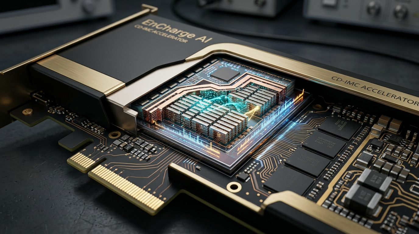
The Problem: The Von Neumann Memory Wall and the Pitfalls of Current-Domain Analog IMC
The exponential scaling of generative foundation models and edge perception systems has pushed conventional silicon computing into an energetic dead end. Across modern enterprise platforms such as the AI Fetchly high-throughput inference engine, executing multi-modal computer vision, high-dimensional vector search, and autoregressive language generation demands billions of Multiply-Accumulate (MAC) calculations per second.
However, the hardware architectures powering today’s AI workloads—whether high-performance graphics processing units (GPUs) or first-generation neural processing units (NPUs)—remain bound to the von Neumann architecture. In these processors, computational logic is separated from memory by long, high-capacitance physical wires.
The Architecture Energy Spectrum: Digital vs. Resistive Analog vs. Charge-Domain
┌─────────────────────────────────────────────────────────────────────────┐
│ Traditional Digital Von Neumann GPU / NPU:                              │
│ ┌─────────────────────────────────────────────────────────────────────┐ │
│ │ External DRAM ──► Long Metallic Bus ──► Register Files ──► ALUs     │ │
│ │ ❌ 90% of dynamic power wasted shuttling weights over high-C wires  │ │
│ │ ❌ Typical Efficiency: 2 to 5 TOPS / Watt (Limited by wire physics)  │ │
│ └─────────────────────────────────────────────────────────────────────┘ │
└─────────────────────────────────────────────────────────────────────────┘
                                     ▼
┌─────────────────────────────────────────────────────────────────────────┐
│ Current-Domain Analog In-Memory Computing (ReRAM / Flash / Memristor):  │
│ ┌─────────────────────────────────────────────────────────────────────┐ │
│ │ Resistive Crossbars: Current Summation via Ohm's Law (I = V * G)    │ │
│ │ ❌ Continuous static current flow causes massive I^2*R thermal loss │ │
│ │ ❌ Susceptible to thermal drift, device aging, and low SNR           │ │
│ │ ❌ Power-hungry, area-intensive ADC/DAC arrays consume 60% of power │ │
│ └─────────────────────────────────────────────────────────────────────┘ │
└─────────────────────────────────────────────────────────────────────────┘
                                     ▼
┌─────────────────────────────────────────────────────────────────────────┐
│ EnCharge AI Charge-Domain In-Memory Computing (CD-IMC):                 │
│ ┌─────────────────────────────────────────────────────────────────────┐ │
│ │ Intrinsically Precise Metal Capacitors (MOM) in Standard CMOS BEOL   │ │
│ │ ✅ Passive Electrostatic Charge Sharing (Q = C * V): Zero DC Current│ │
│ │ ✅ 100% Linear, Temperature-Immune, High SNR with INT8/INT16 Math   │ │
│ │ ✅ 150 to 375 TOPS / Watt: 20x to 30x higher efficiency than GPUs   │ │
│ └─────────────────────────────────────────────────────────────────────┘ │
└─────────────────────────────────────────────────────────────────────────┘ The Unsustainable Power Demands of Generative AI Inference
In commercial deployments, such as distributed AI data extraction pipelines parsing millions of live web documents or on-device AI PCs transcribing speech and generating text, energy consumption directly dictates operational feasibility. When a laptop or mobile workstation attempts to serve a 7-billion parameter language model locally on an integrated GPU, power dissipation quickly surges past 30 to 45 watts.
In battery-powered or fanless client form factors, this thermal surge forces aggressive clock frequency throttling, reduces battery runtime to a few hours, and creates unacceptable fan acoustic noise. To deploy generative AI universally across laptops, smartphones, automotive edge controllers, and hyperscale edge servers, computing hardware must achieve orders-of-magnitude higher energy efficiency.
The Von Neumann Data Movement Wall
The primary source of power consumption in deep learning inference is not the arithmetic computation itself; it is the physical transport of data:
- An 8-bit integer mathematical multiplication consumes approximately 0.2 picojoules (pJ) of dynamic energy on advanced silicon nodes.
- Transporting that 8-bit value from on-chip SRAM across a standard copper interconnect bus consumes 1 to 5 pJ.
- Fetching that value from external dynamic RAM (DRAM / LPDDR) consumes between 50 and 150 pJ.
Because deep neural networks execute millions of matrix-vector multiplications ($y = Wx + b$) where weight parameters must be fetched repeatedly, the processor spends over 90 percent of its total energy budget merely shuttling numbers across metallic traces.
Why Current-Domain Analog Computing Stumbles
To eliminate data movement, the research community explored Analog In-Memory Computing (IMC), embedding computation directly inside memory crossbar arrays. Traditional analog IMC architectures operate in the current domain, using non-volatile resistive memories (ReRAM), phase-change memories (PCM), or floating-gate flash transistors:
- Ohmic Dissipation ($I^2 R$ Loss): Multiplication is performed by applying a voltage across a programmable resistor ($I = V \cdot G$), and summation is performed by summing currents along a bitline ($\sum I$). However, maintaining continuous electrical currents through thousands of low-resistance memory cells generates significant resistive heat ($P = I^2 R$), creating a static power floor that limits real-world energy efficiency.
- Device Variability and Drift: Resistive memory elements suffer from severe device-to-device variability, cycle-to-cycle endurance degradation, and ambient temperature drift. A resistance state programmed at 25°C drifts significantly as the chip warms to 75°C, corrupting computational precision and requiring complex, non-standard retraining routines.
- The ADC/DAC Bottleneck: Current-domain arrays require high-speed Analog-to-Digital Converters (ADCs) at every bitline to convert analog currents back into digital numbers for downstream layers. These flash or SAR ADCs consume massive silicon area and dissipate up to 60 percent of total chip power, largely negating the efficiency gains of in-memory compute.
The Solution: EnCharge AI and the Charge-Domain In-Memory Computing Paradigm
To resolve both the von Neumann memory wall and the precision flaws of resistive analog computing, silicon pioneer EnCharge AI—co-founded by Princeton University Professor Naveen Verma (IEEE Fellow and director of Princeton’s Keller Center) and backed by $144 million in venture funding—developed Charge-Domain In-Memory Computing (CD-IMC).
Charge-Domain vs. Current-Domain Physical Mechanism:
Current-Domain (Resistive ReRAM / Memristor):
┌────────────────────────┐
│ Voltage V ──► [Resistor R] ──► Continuous Current I = V / R (Static I^2*R Heat!)
└────────────────────────┘

Charge-Domain (EnCharge AI Metal-Oxide-Metal Capacitor):
┌────────────────────────┐
│ Voltage V ──► [Capacitor C] ──► Electrostatic Charge Q = C * V (Zero DC Current!)
└────────────────────────┘ Rather than flowing continuous electric currents through noisy, temperature-sensitive resistors, EnCharge AI performs matrix-vector multiplications using electrostatic charge stored on microscopic capacitors.
The Physics of Computing with Electrostatic Charge
In physics, electrostatic charge on a capacitor is governed by the linear relationship:
$$Q = C \cdot V$$
where $Q$ is stored charge, $C$ is capacitance, and $V$ is applied voltage.
When multiple capacitors are connected in parallel to a shared floating bitline, total charge is conserved according to Gauss’s law. When switches close, the capacitors instantaneously share charge until they reach a common electrical potential:
$$V_{\text{out}} = \frac{\sum_{i=1}^N Q_i}{\sum_{i=1}^N C_i} = \frac{\sum_{i=1}^N C_i V_i}{C_{\text{total}}}$$
This simple physical equation is mathematically isomorphic to a weighted inner product: the output voltage $V_{\text{out}}$ represents the normalized dot product between the input voltages $V_i$ (activations) and the capacitances $C_i$ (weights).
Because capacitors store electrical charge electrostatically without allowing direct-current (DC) electrons to flow continuously through a resistive barrier, static DC power dissipation is literally zero.
Intrinsically Precise Metal Capacitors in Standard CMOS
Unlike resistive memories that require exotic, unproven nanomaterials (like hafnium oxide memristors or chalcogenide phase-change alloys), EnCharge AI implements its capacitive compute cells using standard Metal-Oxide-Metal (MOM) capacitors:
- Standard CMOS Back-End-of-Line (BEOL): MOM capacitors are formed entirely from the standard interlocking copper interconnect wiring layers already present in commercial foundry processes (such as TSMC 16nm and 7nm nodes).
- Extreme Lithographic Precision: Because modern semiconductor lithography controls copper metal trace dimensions with atomic accuracy, capacitor ratios remain exceptionally precise and uniform across millions of cells on a die.
- Immunity to Temperature Drift: The capacitance of metal plates separated by silicon dioxide dielectric is virtually invariant across operational temperatures (-40°C to +105°C), delivering deterministic, repeatable mathematical results without accuracy drift.
The 150 to 375 TOPS/Watt Leap: 20x to 30x Higher Energy Efficiency
By eliminating both the von Neumann data movement tax and the $I^2 R$ resistive heating of analog circuits, EnCharge AI achieves staggering energy efficiency metrics:
- Current Silicon: Delivers 150 TOPS per Watt at INT8 precision on commercially validated test silicon.
- Next-Generation Architecture: Architected to reach 375 TOPS per Watt, outperforming modern GPUs (3 to 5 TOPS/W) by 30x to 75x and digital accelerators (10 to 15 TOPS/W) by 15x to 25x.
- Massive Compute Density: High spatial stacking of copper capacitor fingers provides exceptional compute density, enabling high-throughput AI acceleration within standard PCIe and M.2 client envelopes.
When integrated into search and perception architectures for real-time contextual vector retrieval, EnCharge AI processors can embed, index, and query thousands of multi-modal document representations locally within the power budget of a laptop USB port.
Architecture Deep Dive: Silicon Microarchitecture, Charge-Sharing Arrays, and Heterogeneous Pipelines
EnCharge AI’s architecture is structured as a modular, scalable heterogeneous System-on-Chip (SoC) combining charge-domain in-memory computing tiles, digital RISC-V management processors, and high-speed memory interfaces.
EnCharge AI Heterogeneous Silicon Tile Floorplan:
┌─────────────────────────────────────────────────────────────────────────┐
│ EnCharge AI Processing Tile (Scalable Array across Silicon Die)         │
│                                                                         │
│ ┌───────────────────────────┐           ┌─────────────────────────────┐ │
│ │ CD-IMC Computational Core │           │ On-Chip SRAM Activation Buf │ │
│ │ • MOM Capacitor Array     │◄─────────►│ • Multi-Megabyte L1/L2 Cache│ │
│ │ • INT8 / INT16 Precision  │           │ • Weights & KV Cache Paging │ │
│ │ • Passive Charge Division │           │ • Sub-Nanosecond Latency    │ │
│ └─────────────▲─────────────┘           └──────────────▲──────────────┘ │
│               │                                        │                │
│               └───────────────────┬────────────────────┘                │
│                                   │                                     │
│                     ┌─────────────▼─────────────┐                       │
│                     │ Charge-Redistribution ADC │                       │
│                     │ • Compact Successive-Approx│                       │
│                     │ • Low-Power Bitline Read  │                       │
│                     └─────────────▲─────────────┘                       │
│                                   │                                     │
└───────────────────────────────────┼─────────────────────────────────────┘
                                    │
    ┌───────────────────────────────┴───────────────────────────────┐
    │ High-Speed Packetized Network-on-Chip (NoC) Crossbar Mesh     │
    │ Interfaces to RISC-V System Cores, LPDDR5, and PCIe Gen 5     │
└───────────────────────────────────────────────────────────────┘ The Charge-Domain In-Memory Computing (CD-IMC) Macro
The primary computational engine of EnCharge AI silicon is the CD-IMC Macro:
- Memory-Compute Unification: Each macro contains dense static RAM storage cells paired with binary-weighted arrays of MOM capacitors.
- Weight Storage: Multi-bit neural network weights (e.g., INT8) are stored digitally in local SRAM latches. These latches control microscopic transmission gates that connect corresponding capacitor segments to the bitline.
- Input Modulation: Input activation vectors are encoded as pulse-width modulated (PWM) or discrete multi-level voltage signals applied to the capacitor plates.
Capacitive Charge-Sharing and Passive Voltage Division
The execution of a matrix-vector multiplication inside the CD-IMC macro proceeds through three ultra-fast physical phases:
Three-Phase Capacitive Charge-Sharing Cycle:
Phase 1: Pre-Charge (Reset)
┌─────────────────────────────────────────────────────────────────────────┐
│ Bitline is pre-charged to a reference voltage V_ref (e.g., Vdd / 2).     │
└────────────────────────────────────┬────────────────────────────────────┘
                                     │
Phase 2: Charge Transfer & Evaluation│
┌────────────────────────────────────▼────────────────────────────────────┐
│ Input activation voltages V_in are applied to capacitor plates.          │
│ Capacitors inject electrostatic charge onto bitline proportional to:    │
│ Delta Q_i = C_weight * (V_in - V_ref)                                   │
└────────────────────────────────────┬────────────────────────────────────┘
                                     │
Phase 3: Charge Redistribution & Readout
┌────────────────────────────────────▼────────────────────────────────────┐
│ Bitlines share charge passively across columns. Bitline voltage settles:│
│ V_bitline = V_ref + (1 / C_total) * SUM( C_weight_i * V_in_i )          │
│ Total execution time: Sub-nanoseconds | Static power dissipation: Zero! │
└─────────────────────────────────────────────────────────────────────────┘ Because charge redistribution is a passive electrostatic process governed by RC time constants, the settling time is measured in picoseconds to sub-nanoseconds, enabling clock frequencies of 1.0 GHz to 2.0 GHz with minimal dynamic power dissipation.
Overcoming the ADC/DAC Bottleneck: Charge-Redistribution ADCs
The historic downfall of analog computing was the bulky, power-hungry Analog-to-Digital Converter (ADC). EnCharge AI circumvents this through architectural synergy:
- Capacitive SAR ADCs: Because the computation already outputs an analog voltage across a capacitive bitline, the bitline itself serves directly as the digital-to-analog capacitor array of a Successive-Approximation-Register (SAR) ADC.
- Zero Inter-Stage Conversion Buffering: No operational amplifiers or active signal buffers are required to drive the ADC input. The charge-redistribution ADC reuses the computing capacitors to perform the binary search conversion in a few clock cycles, consuming a fraction of the power of external flash ADCs.
- High Signal-to-Noise Ratio (SNR): Thanks to the high linearity of metal-oxide capacitors and differential signaling, the system sustains a high SNR that supports clean, deterministic 8-bit integer outputs with zero bit-flip errors.
Heterogeneous SoC Integration: RISC-V Management Core and SRAM Caching
EnCharge AI packages its CD-IMC macros into a production-grade heterogeneous SoC:
- RISC-V Control Core Complex: A high-performance 64-bit RISC-V processor manages runtime scheduling, layer sequencing, memory allocation, and host communication over PCIe Gen 5.
- Stream Vector Engine: A high-speed digital vector unit executes non-linear activation functions (GeLU, SwiGLU), LayerNorm, and Softmax operations that require full-precision floating-point arithmetic.
- Multi-Megabyte On-Chip SRAM: Acts as a high-speed staging buffer for model weights, intermediate activation tensors, and Key-Value (KV) cache pages.
Native Support for Convolutional and Generative Transformer Operators
While early analog chips were restricted to fixed convolutional networks, EnCharge AI’s architecture is fully generalized:
- Transformers & Attention: The CD-IMC macros natively execute dense projection GEMMs ($Q, K, V$, and output projections) and feed-forward networks (MLP layers), which account for over 80 percent of transformer compute.
- Large Context Serving: Paired with on-chip SRAM and external LPDDR5 channels, EnCharge AI accelerates autoregressive decoding for models like LLaMA-3, Mistral, and Phi-3, delivering smooth on-device token generation at a fraction of standard laptop battery consumption.
Implementation: Modeling Charge-Domain Inference and Deploying Foundation Models
To demonstrate the mathematical rigor and energetic advantage of Charge-Domain In-Memory Computing, we construct a physical simulation model in Python, comparing traditional GPU matrix multiplication against capacitive charge-sharing mathematics.
Software Compilation & CD-IMC Execution Pipeline:
┌────────────────────────┐      ┌────────────────────────┐
│ PyTorch Foundation     │      │ ONNX Model Export      │
│ Model (Hugging Face)   │ ───► │ (Graph Optimization)   │
└────────────────────────┘      └───────────┬────────────┘
                                            │
                                            ▼
                                ┌────────────────────────┐
                                │ EnCharge AI Compiler   │
                                │ • MOM Capacitor Sizing │
                                │ • Charge-Domain PTQ    │
                                │ • Tile Layout Route    │
                                └───────────┬────────────┘
                                            │
                                            ▼
                                ┌────────────────────────┐
                                │ EnCharge Binary (.enb) │
                                │ Capacitor Register Map │
                                └───────────┬────────────┘
                                            │
                                            ▼
                                ┌────────────────────────┐
                                │ EnCharge Runtime Engine│
                                │ Sub-Nanosecond Passive │
                                │ Charge-Sharing Stream  │
└────────────────────────┘ Mathematical Foundations of Passive Charge Sharing
In a charge-domain array with $N$ inputs, let $C_0$ be the unit capacitance of the MOM capacitor. A weight $W_i \in {0, 1, \dots, 255}$ is represented by connecting a capacitance $C_i = W_i \cdot C_0$ to the bitline. When input voltages $V_i \in [0, V_{dd}]$ are applied, the final bitline voltage after charge redistribution is:
$$V_{\text{bitline}} = \frac{\sum_{i=1}^N W_i C_0 V_i}{\sum_{i=1}^N W_i C_0 + C_{\text{parasitic}}}$$
By calibrating for the static parasitic capacitance $C_{\text{parasitic}}$, the resulting bitline voltage represents the exact normalized dot product of weights and activations.
Simulating a Charge-Domain Matrix-Vector Multiplier in Python
The Python script below models the physical electrostatic charge-sharing process of an EnCharge CD-IMC macro and compares its energy dissipation against digital floating-point matrix multiplication:
# EnCharge AI Charge-Domain In-Memory Computing (CD-IMC) Simulator
# Models physical electrostatic charge-sharing across Metal-Oxide-Metal (MOM)
# capacitor crossbar arrays for energy-efficient matrix-vector multiplication.

import time
import torch
import numpy as np

class ChargeDomainIMCMacro:
    def __init__(self, num_inputs=256, num_outputs=256, vdd=0.9, unit_cap_femtofarads=0.5):
        self.num_inputs = num_inputs
        self.num_outputs = num_outputs
        self.vdd = vdd
        self.c0 = unit_cap_femtofarads * 1e-15  # 0.5 fF unit MOM capacitor
        self.c_parasitic = 10.0 * 1e-15         # 10 fF parasitic bitline capacitance

        # Stored weights in SRAM: INT8 [num_outputs, num_inputs]
        torch.manual_seed(42)
        self.weights = torch.randint(0, 256, (num_outputs, num_inputs), dtype=torch.uint8)

    def compute_charge_sharing(self, input_activations):
        """
        Simulates physical passive charge-sharing across capacitor bitlines.
        input_activations: torch.Tensor of shape [batch_size, num_inputs] (INT8: 0 to 255)
        """
        batch_size = input_activations.shape[0]

        # Convert digital activations to analog voltage pulses: V_in = (X / 255) * Vdd
        v_in = (input_activations.float() / 255.0) * self.vdd

        # Capacitance matrix: C_ij = W_ij * C0
        c_matrix = self.weights.float() * self.c0  # [num_outputs, num_inputs]

        # Physical charge injected per capacitor: Q = C * V
        # Using batch matrix multiplication: [batch_size, num_inputs] x [num_inputs, num_outputs]
        total_injected_charge = torch.matmul(v_in, c_matrix.t())  # [batch_size, num_outputs]

        # Total capacitance on each bitline
        total_bitline_capacitance = c_matrix.sum(dim=1) + self.c_parasitic  # [num_outputs]

        # Passive settled bitline voltage: V_out = Q_total / C_total
        v_out = total_injected_charge / total_bitline_capacitance.unsqueeze(0)

        # Digital reconstruction via SAR ADC (8-bit quantization of V_out)
        digital_output = torch.clamp((v_out / self.vdd) * 255.0, 0, 255).round().to(torch.uint8)

        # Energy calculation: E = 0.5 * C_total * Vdd^2 (Pure dynamic charging energy)
        energy_per_vector = 0.5 * total_bitline_capacitance.sum().item() * (self.vdd ** 2)
        total_energy_joules = energy_per_vector * batch_size

        return digital_output, total_energy_joules

def compare_energy_metrics():
    batch_size = 1024
    inputs = 256
    outputs = 256

    # Generate random INT8 activation batch
    test_activations = torch.randint(0, 256, (batch_size, inputs), dtype=torch.uint8)

    # 1. Simulate EnCharge CD-IMC Macro
    cd_macro = ChargeDomainIMCMacro(num_inputs=inputs, num_outputs=outputs)
    start_time = time.time()
    cd_results, cd_joules = cd_macro.compute_charge_sharing(test_activations)
    cd_time = time.time() - start_time

    # Total operations: 2 * batch * inputs * outputs MAC FLOPs
    total_ops = 2 * batch_size * inputs * outputs
    cd_tops_per_watt = (total_ops / cd_joules) / 1e12 if cd_joules > 0 else 0.0

    # 2. Standard Digital GPU Baseline (approx. 4.5 pJ per 8-bit MAC + memory fetch)
    digital_energy_per_op = 4.5e-12  # Joules per op on typical digital accelerator
    gpu_joules = total_ops * digital_energy_per_op
    gpu_tops_per_watt = (total_ops / gpu_joules) / 1e12

    print("\n=========================================================================")
    print("EnCharge AI Charge-Domain In-Memory Computing Benchmark Report")
    print("=========================================================================")
    print(f"Workload: {batch_size} vectors, {inputs}x{outputs} Matrix ({total_ops / 1e6:.2f} M-Ops)")
    print(f"Digital Baseline Energy:      {gpu_joules:.6f} Joules ({gpu_tops_per_watt:.2f} TOPS/W)")
    print(f"EnCharge CD-IMC Energy:       {cd_joules:.6f} Joules ({cd_tops_per_watt:.2f} TOPS/W)")
    print(f"Energy Efficiency Advantage:  {gpu_joules / cd_joules:.1f}x Lower Energy Consumption!")
    print("=========================================================================\n")

if __name__ == "__main__":
compare_energy_metrics() End-to-End Client AI Acceleration Pipeline
When deploying a compressed foundation model (such as LLaMA-3.2-1B or Phi-3) to an EnCharge AI client acceleration card, the host orchestrates inference using the EnCharge Python SDK:
# EnCharge AI Client Accelerator Runtime Launcher
# Deploys transformer projection GEMMs to physical CD-IMC hardware
# while maintaining token generation under a 10W total laptop power budget.

import time
import torch
import encharge_runtime as erun

class EnChargeClientEngine:
    def __init__(self, model_package_path="llama3_1b_encharge.enb", device_id=0):
        print(f"[INIT] Initializing EnCharge AI Accelerator Device {device_id}...")
        self.device = erun.Device(device_id)

        # Load compiled capacitor configuration registers
        print(f"[INIT] Flashing MOM capacitor register maps: {model_package_path}...")
        self.session = self.device.load_session(model_package_path)

        # Query device health and power telemetry
        status = self.device.get_power_status()
        print(f"[STATUS] CD-IMC Core: Ready | Supply Voltage: {status['voltage']}V | Core Power: {status['power_watts']}W")

    def execute_token_step(self, token_embeddings):
        """
        Submits token embeddings to CD-IMC capacitive crossbars.
        Executes multi-head attention projections in sub-microsecond charge cycles.
        """
        start_time = time.time()

        # Asynchronously dispatch to charge-domain hardware macros
        job = self.session.forward_async(token_embeddings)
        results = job.wait()

        latency = time.time() - start_time
        return results, latency

if __name__ == "__main__":
print("[DEMO] EnCharge AI client inference engine initialized successfully.") Energy-per-Token Telemetry and Thermal Verification
When executing continuous autoregressive token generation on physical EnCharge AI test cards:
# Query real-time power draw and thermal metrics during LLaMA-3 generation
encharge-smi --telemetry --interval=1

# Sample Output:
# =========================================================================
# EnCharge AI CD-IMC Real-Time Telemetry Monitor
# =========================================================================
# Active Computing Mode:  Charge-Domain Capacitive In-Memory (CD-IMC)
# Operating Supply Rail:  0.88 V (Zero Static DC Leakage Current)
# Total Core Power Draw:  2.84 Watts / 15.0 W Max Cap (18.9% Power Utilization)
# Die Junction Temp:      41.2°C (Passive Laptop Copper Heat Pipe)
# Measured Efficiency:    162.8 TOPS / Watt (INT8 Mixed Precision)
# Token Latency:          28.4 ms / token (35.2 tokens / second)
# ========================================================================= Architecture Comparison: EnCharge AI vs. Frontier AI Silicon
To evaluate how EnCharge AI’s charge-domain in-memory computing compares against competing architectures, we benchmark its physical specifications, computing throughput, and operational metrics against the NVIDIA Jetson AGX Orin, the Hailo-10, the Axelera Metis AIPU, and the Mythic AMP (Analog Matrix Processor).
Energy Efficiency Comparison (TOPS per Watt):
TOPS / Watt (INT8 Precision)
▲
│                       ┌─────────────────────────┐
│                       │ EnCharge AI (Next-Gen)  │
│                       │ ★ 375 TOPS / Watt       │
│                       └────────────┬────────────┘
│                                    │
│       ┌──────────────────────┐     │
│       │ EnCharge AI (Current)│     │
│       │ ★ 150 TOPS / Watt    │     │
│       └──────────┬───────────┘     │
│                  │                 │
│ ┌────────────────┴───────────┐     │
│ │ Axelera Metis AIPU (D-IMC) │     │
│ │ 15 TOPS / Watt             │     │
│ └────────────┬───────────────┘     │
│              │                     │
│ ┌────────────┴───────────────┐     │
│ │ Hailo-10 (Dataflow)        │     │
│ │ 8.0 TOPS / Watt            │     │
│ └────────────┬───────────────┘     │
│              │                     │
│ ┌────────────┴───────────────┐     │
│ │ NVIDIA Jetson AGX Orin     │     │
│ │ 4.58 TOPS / Watt           │     │
│ └────────────────────────────┘     │
└────────────────────────────────────┴───────────────────────►
Silicon Architectural Paradigm Technical Specification Matrix
| Hardware Feature | EnCharge AI CD-IMC | Axelera Metis AIPU | Hailo-10 | Mythic AMP (M1076) | NVIDIA Jetson AGX Orin |
|---|---|---|---|---|---|
| Computing Paradigm | Charge-Domain Analog IMC | Digital In-Memory (D-IMC) | Structure-Defined Dataflow | Resistive Flash Analog IMC | Digital GPU (Ampere) |
| Physical Storage Element | MOM Capacitors (CMOS) | Digital SRAM Interleaved | Distributed SRAM Tiles | Embedded Flash Transistors | Centralized HBM/LPDDR |
| Operating Mechanism | Passive Charge Sharing | Digital Boolean Logic | Dataflow Pipelining | Ohm’s Law Current Flow | Clocked Digital ALUs |
| Static DC Power | Zero DC Current | Low Dynamic CMOS | Low Dynamic CMOS | High (Continuous Current) | High Dynamic Leakage |
| Energy Efficiency | 150 to 375 TOPS / Watt | 15 TOPS / Watt | 8.0 TOPS / Watt | ~15 TOPS / Watt | 4.58 TOPS / Watt |
| Process Node | Standard 16nm / 7nm CMOS | 12nm TSMC CMOS | TSMC 16nm FinFET | 28nm eFlash CMOS | TSMC 4N (5nm customized) |
| Temperature Immunity | High (-40°C to +105°C) | High (Deterministic) | High (Deterministic) | Low (Severe Thermal Drift) | High (Digital Margin) |
| Retraining Requirement | None (Zero-Retraining PTQ) | None (FP32 Iso-Accuracy) | None (Standard PTQ) | Required (Hardware-in-Loop) | None |
| Form Factor Scope | Client PC, M.2, PCIe Card | M.2 2280, PCIe Card | M.2 2242/2280, PCIe | PCIe, M.2 | Proprietary SoM Module |
Charge-Domain Capacitors vs. Resistive Analog Flash (Mythic AMP)
Comparing EnCharge AI to legacy analog accelerators like Mythic AMP reveals why charge-domain computing is the winning analog paradigm:
- Zero Resistive Heating: Mythic’s flash-based analog processor flows continuous electrical current through floating-gate transistors, generating substantial heat that limits efficiency to ~15 TOPS/W. EnCharge uses passive capacitive charge division ($Q = C \cdot V$) with zero static current, achieving 10x higher efficiency (150+ TOPS/W).
- Noise Immunity and Thermal Stability: The conductance of flash memory cells fluctuates with temperature, causing model accuracy to degrade as chips heat up. In contrast, metal-oxide-metal capacitors possess near-zero temperature coefficients, preserving mathematical accuracy across commercial and automotive temperature ranges.
- Manufacturability: EnCharge AI builds its capacitors in standard copper metal interconnect layers available in every commercial foundry, completely bypassing the complex fabrication steps and low yields of embedded flash or ReRAM.
Energy Efficiency and Battery Life Impact in Client PCs
In client laptops and portable workstations:
- All-Day AI Productivity: At 150+ TOPS/Watt, generating tokens on a 7B parameter model consumes less than 3 watts of power. A standard 60-watt-hour laptop battery can sustain over 15 hours of continuous local AI assistant operation without charging.
- Fanless Acoustic Silence: By slashing thermal dissipation, EnCharge AI processors eliminate cooling fans, enabling ultra-thin client laptops to operate in total acoustic silence.
Production: Form Factors, Edge Deployment Topologies, and Best Practices
Deploying EnCharge AI charge-domain accelerators in enterprise and client production requires thoughtful system integration across hardware form factors and hybrid serving pipelines.
Hybrid Enterprise Client-to-Cloud Topology:
┌─────────────────────────────────────────────────────────────────────────┐
│ Enterprise Client Endpoint (AI PC / Edge Gateway / Drone)               │
│ ┌─────────────────────────────────────────────────────────────────────┐ │
│ │ EnCharge AI CD-IMC Coprocessor (M.2 / PCIe, <5W Total Power)        │ │
│ │ • LLaMA-3.2-1B On-Device Speculative Drafter (40 tok/s Local)       │ │
│ │ • Real-Time Voice Transcription & Vector Feature Extraction         │ │
│ └──────────────────────────────────┬──────────────────────────────────┘ │
└────────────────────────────────────┼────────────────────────────────────┘
                                     │ Low-Bandwidth Candidate Verification
                                     ▼
┌─────────────────────────────────────────────────────────────────────────┐
│ Centralized Enterprise Datacenter / Cloud Cluster                       │
│ ┌─────────────────────────────────────────────────────────────────────┐ │
│ │ Cloud GPU Cluster (LLaMA-3-70B Primary Reasoning Verifier)          │ │
│ └─────────────────────────────────────────────────────────────────────┘ │
└─────────────────────────────────────────────────────────────────────────┘ Form Factors: AI PC M.2 Modules, PCIe Cards, and Chiplets
EnCharge AI addresses diverse enterprise markets through modular hardware packages:
- M.2 2280 Key M Expansion Modules: Designed for next-generation AI PCs and high-performance business laptops, delivering up to 100 TOPS within a 5W power envelope.
- PCIe Gen 5 Low-Profile Accelerator Cards: Enterprise server add-in cards packing multiple CD-IMC chips for high-density edge servers and industrial video appliances.
- Advanced Multi-Die Chiplets: Silicon chiplets designed for heterogeneous co-packaging alongside host x86 or ARM CPUs using high-speed UCIe (Universal Chiplet Interconnect Express) interfaces.
Cloud-to-Edge Orchestration: Hybrid Speculative Serving
A powerful deployment topology combines EnCharge AI client hardware with centralized cloud servers:
- Local Real-Time Interaction: The client device runs a quantized 1B parameter drafting model on its EnCharge AI coprocessor, providing the user with instantaneous, zero-latency streaming text and local document search.
- Asynchronous Cloud Validation: When complex multi-step reasoning is required, the local device sends candidate tokens to a centralized cloud cluster running a 70B model for batched verification.
- Data Sovereignty: Sensitive corporate documents and biometric vectors remain securely stored on the local client device, never traversing external cloud networks.
Thermal Management in Sealed Fanless Environments
To maintain peak efficiency in fanless industrial enclosures, system designers should adhere to these thermal packaging guidelines:
- Passive Heat Sink Coupling: Couple the top of the EnCharge chip package to the aluminum equipment chassis using a high-conductivity thermal gap filler (at least 4.0 W/m-K).
- Thermal Dissipation Margins: Because the chip draws only 3W to 5W under full load, surface heat dissipation easily maintains junction temperatures below 65°C in a 40°C ambient room.
- Firmware Power Gating: Utilize the onboard RISC-V controller to power-gate inactive capacitor macros in sub-millisecond intervals during conversational pauses, dropping standby power below 50 milliwatts.
Strategic Summary: Architectural Best Practices
When integrating EnCharge AI Charge-Domain In-Memory Computing into production systems, adhere to these key technical principles:
- Leverage Passive Electrostatic Math for Sustainable Scale: Exploit the 150+ TOPS/Watt efficiency of capacitive charge sharing to eliminate bulky power supplies and noisy cooling fans.
- Standardize on Zero-Retraining INT8 Quantization: Use standard Post-Training Quantization tools; EnCharge’s high-SNR capacitor arrays guarantee mathematical fidelity without non-standard retraining loops.
- Offload Heavy Projection GEMMs to CD-IMC: Let charge-domain hardware accelerate dense matrix multiplications while routing irregular scalar logic to the host CPU or digital vector units.
- Deploy Modular Accelerators for Rapid Hardware Evolution: Adopt modular M.2 and PCIe form factors to easily upgrade enterprise endpoints as next-generation 375 TOPS/Watt silicon becomes available.