DeepX DX-M1 Guide: 5nm 25-TOPS Sub-5W Edge AI NPU Silicon
The Thermal and Memory Wall in Edge AI Acceleration
Deploying modern computer vision and multi-modal neural network architectures to edge devices has historically presented a severe engineering dilemma. Edge computing environments—such as autonomous mobile robots, automated optical inspection cameras on smart factory conveyor lines, drone navigation pods, and roadside traffic management units—operate under unforgiving physical constraints. These deployments cannot accommodate active liquid cooling manifolds, noisy high-RPM chassis fans, or bulky multi-hundred-watt power supplies. Engineers are bound by a strict thermal dissipation envelope of under 5 to 10 watts total board power while requiring sustained, real-time throughput across dozens of concurrent high-definition video streams.
For years, system architects have relied on general-purpose GPU microarchitectures or legacy neural compute sticks. However, conventional embedded GPUs inherit fundamental architectural limitations from their desktop and datacenter lineage. First, traditional architectures dedicate massive die real estate to hardware graphics pipelines, complex floating-point texture units, and multi-level cache hierarchies designed for speculative execution rather than deterministic tensor contractions. Second, and more critically, standard embedded accelerators suffer from catastrophic memory bus bottlenecks, commonly referred to as the memory wall.
When executing dense convolutional neural networks or vision transformers, transferring billions of weight parameters and intermediate feature maps between off-chip DRAM and the on-chip arithmetic logic units consumes significantly more energy per operation than the arithmetic calculation itself. In typical edge devices equipped with narrow 32-bit or 64-bit LPDDR4 memory buses, DRAM access accounts for 60% to 80% of total subsystem power dissipation. As a consequence, attempting to process 16 to 32 streams of 1080p video at 30 frames per second on legacy edge hardware rapidly triggers thermal throttling, drops frames, introduces unacceptable inference tail latency, and degrades operational reliability.
Furthermore, post-training quantization has historically compromised model accuracy. While INT8 or INT4 quantization reduces DRAM bandwidth and compute overhead, aggressive uniform quantization across deep networks frequently leads to severe precision degradation in sensitive layers, such as depthwise separable convolutions, multi-head self-attention projections, and regression bounding-box heads. Developers have been forced to choose between fast but inaccurate quantized models and accurate but thermally unmanageable floating-point execution. The industry requires an entirely rethought silicon architecture: an application-specific neural processing unit fabricated on advanced semiconductor nodes that eliminates off-chip DRAM latency penalties, delivers true sub-5W power efficiency, and preserves near-lossless floating-point accuracy.
Introducing DeepX DX-M1: 5nm Silicon for Fanless Edge Intelligence
The DeepX DX-M1 emerges as an uncompromising architectural solution to edge inference bottlenecks. Conceived and engineered by South Korean fabless semiconductor pioneer DEEPX—led by former Apple lead application processor designer Lokwon Kim—the DX-M1 is an ultra-low-power, high-performance Neural Processing Unit (NPU) accelerator engineered from the ground up for embedded and edge enterprise intelligence. Fabricated on Samsung Foundry’s advanced 5nm FinFET process node, the DX-M1 packs 25 trillion operations per second (TOPS) of raw INT8 computing capability into a power envelope operating between 3W and 5W typical consumption.
To overcome the edge memory wall, the DX-M1 introduces a clean-slate, streaming spatial dataflow architecture coupled with patented ultra-low-bit precision quantization algorithms. Unlike conventional compute architectures that continuously shuttle intermediate activations back and forth across an external memory bus, the DX-M1 utilizes a Zero-DRAM latency dataflow engine. Intermediate layer outputs remain pinned within high-density on-chip static RAM (SRAM) memory banks, streaming directly into subsequent computational stages through dedicated spatial pipelines. This design reduces external memory access cycles by more than an order of magnitude, drastically lowering dynamic switching power and thermal dissipation.
Complementing its hardware architecture, the DX-M1 is supported by the DXNN software development kit and compilation framework. DXNN features an automated, patent-backed hybrid quantization engine capable of converting full-precision FP32 models into optimized INT8 and mixed-precision representations while maintaining greater than 99% iso-accuracy relative to baseline floating-point models. Packaged in a compact M.2 2280 (M-key and B+M key) form factor equipped with up to 4GB of LPDDR5 memory, the DX-M1 integrates seamlessly into industrial PCs, edge servers, smart camera gateways, and robotics controller platforms via high-speed PCIe Gen3 x4 interfaces.
Architects integrating automated vision pipelines with edge data collection can connect their edge nodes to centralized platforms using distributed data-fetching pipelines to synchronize metadata, model weights, and telemetry across edge-to-cloud topologies. Whether deployed on factory floors inspecting precision microelectronics or embedded inside intelligent traffic intersections, the DX-M1 provides deterministic, ultra-low-latency neural acceleration without requiring active cooling fans or external cooling assemblies.
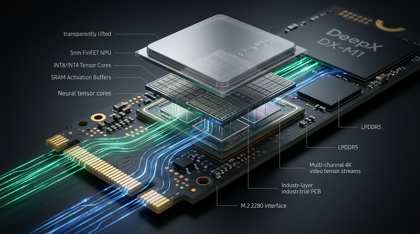
Architectural Deep Dive: Samsung 5nm FinFET, Processing Elements, and Zero-DRAM Latency
Understanding the exceptional performance-per-watt metric of the DeepX DX-M1 requires an examination of its microarchitecture across four primary subsystems: the Samsung 5nm FinFET physical design, the tiled Processing Element (PE) matrix, the on-chip streaming SRAM interconnect, and the integrated host interface.
Samsung 5nm FinFET Physical Implementation and Power Domains
The physical realization of the DX-M1 on Samsung Foundry’s 5nm FinFET semiconductor node provides fundamental density and electrostatic gate control advantages over legacy 12nm, 16nm, or 28nm edge silicon. The 5nm process node employs extreme ultraviolet (EUV) lithography to achieve tight transistor pitch scaling, reducing parasitics and gate capacitance. The DX-M1 die architecture is partitioned into independent voltage and frequency power islands:
- NPU Core Matrix Island: Contains the primary tensor contraction engines and vector execution units, operating on dynamic voltage and frequency scaling (DVFS) between 600 MHz and 1.0 GHz depending on real-time thermal headroom and workload intensity.
- On-Chip Memory & Fabric Island: Hosts the high-density distributed SRAM macro arrays and ultra-low-latency on-chip crossbar network, maintaining consistent low-voltage operation to safeguard memory cell stability.
- I/O & Memory Controller Island: Interfaces with the 4GB LPDDR5-5500 external memory subsystem across a 32-bit channel and manages the PCIe Gen3 x4 host interconnect, featuring autonomous power gating when the bus enters idle or low-bandwidth states.
Under typical inference workloads—such as running a YOLOv8x object detection network at 60 FPS—the entire DX-M1 chip dissipates between 3.2W and 4.8W. Even under worst-case synthetic stress benchmarks saturating all tensor units simultaneously, peak board dissipation remains safely below 6.5W, enabling passive heat-sink convection cooling in fanless chassis enclosures rated for industrial -20°C to +70°C operating environments.
The Tiled Processing Element (PE) Matrix and Spatial Execution
At the core of the DX-M1 compute engine is a modular, two-dimensional array of specialized Processing Elements (PEs). Each individual PE contains a tightly coupled grid of multiply-accumulate (MAC) units optimized for INT8, INT4, and FP16 operations. Rather than utilizing a traditional SIMD (Single Instruction, Multiple Data) or GPU-style warp scheduler, the DX-M1 implements a spatial computing execution paradigm:
+-----------------------------------------------------------------------+
|                         DeepX DX-M1 Die Topology                      |
+-----------------------------------------------------------------------+
|  +------------------------+  +-------------------------------------+  |
|  | Host Interface Subsys  |  |      LPDDR5 Memory Subsystem        |  |
|  | PCIe Gen3 x4 Controller|  |  4GB LPDDR5-5500 (22 GB/s Bandwidth)|  |
|  +-----------+------------+  +------------------+------------------+  |
|              |                                  |                     |
|  +-----------v----------------------------------v------------------+  |
|  |           High-Bandwidth On-Chip Network-on-Chip (NoC)          |  |
|  +-----------------------------------------------------------------+  |
|        |                  |                  |                  |     |
|  +-----v-----+      +-----v-----+      +-----v-----+      +-----v-----+  |
|  | PE Tile 0 |      | PE Tile 1 |      | PE Tile 2 |      | PE Tile 3 |  |
|  | [128 MACs]|      | [128 MACs]|      | [128 MACs]|      | [128 MACs]|  |
|  | Local SRAM|      | Local SRAM|      | Local SRAM|      | Local SRAM|  |
|  +-----------+      +-----------+      +-----------+      +-----------+  |
|        ^                  ^                  ^                  ^     |
|  +-----+------------------+------------------+------------------+--+  |
|  |        Zero-DRAM Latency Streaming Activation & Weight Fabric    |  |
|  +-----------------------------------------------------------------+  |
|  |        Hardware Activation Engine (ReLU, GELU, SiLU, Softmax)   |  |
|  +-----------------------------------------------------------------+  |
|  |        Format Converter & Quantization De-quantization Unit     |  |
+--+-----------------------------------------------------------------+--+ Each PE tile is equipped with autonomous hardware micro-sequencers that stream weights and input activations across adjacent PEs via systolic data propagation. Weights can be held stationary in local register files (Weight-Stationary mode) while activations flow horizontally across the tile grid, or intermediate activations can be held stationary (Output-Stationary mode) while weights are broadcast. This dynamic reconfigurability allows the compiler to tailor the execution dataflow to the structural dimensions of each individual layer—maximizing compute utilization whether calculating 1x1 point-wise convolutions, 3x3 depth-wise convolutions, or large multi-head attention matrix multiplications ($Q \times K^T$).
Zero-DRAM Latency Dataflow and Memory Hierarchy
The defining microarchitectural innovation of the DX-M1 is its Zero-DRAM latency streaming technology. In conventional AI chips, when layer $N$ completes execution, its output feature maps are serialized, formatted, and written across the off-chip memory controller into external DRAM. When layer $N+1$ begins, the accelerator halts or stalls until those feature maps are fetched back across the DRAM bus into internal registers. This round-trip latency introduces hundreds of nanoseconds of stall cycles and wastes precious milliwatts of power.
The DX-M1 circumvents this bottleneck by incorporating a massive distributed on-chip SRAM pool configured as an elastic, circular streaming buffer. When layer $N$ computes its output activations, the results are immediately directed into an on-chip channel buffer connected directly to the input ports of the PE tiles assigned to layer $N+1$. Layer $N+1$ begins processing the earliest output tiles of layer $N$ before layer $N$ has even finished computing the entire tensor volume.
By pipelining inter-layer data transfers strictly within on-chip silicon, the external LPDDR5 memory is accessed exclusively for loading the initial model weights upon graph initialization and fetching external video frame buffers from the host PCIe interface. Once loaded, the execution pipeline operates with near-zero off-chip DRAM latency penalties, yielding remarkable computational throughput and deterministic sub-millisecond latencies.
Mathematical Foundations of DeepX Hybrid Quantization
Quantization in the DX-M1 is not an afterthought; it is embedded directly into the arithmetic microarchitecture. To achieve greater than 99% accuracy retention compared to floating-point baselines, DeepX utilizes an advanced hybrid quantization scheme that adaptively applies asymmetric integer quantization where required while minimizing clipping errors.
For an arbitrary weight or activation tensor $X \in \mathbb{R}^{B \times C \times H \times W}$, uniform affine quantization maps continuous floating-point values into an $b$-bit integer representation $q \in [q_{min}, q_{max}]$ according to:
$$q = \text{clamp}\left(\left\lfloor \frac{X}{S} \right\rceil + Z, q_{min}, q_{max}\right)$$
where $S$ represents the positive real-valued quantization scale factor and $Z$ represents the integer zero-point offset:
$$S = \frac{X_{max} - X_{min}}{q_{max} - q_{min}}, \quad Z = \text{round}\left(-X_{min} \cdot \frac{q_{max} - q_{min}}{X_{max} - X_{min}}\right)$$
When multiplying quantized input activations $X_q$ and weight matrices $W_q$, the true mathematical product is recovered in the accumulation pipeline by factoring out the respective scales:
$$\hat{Y} = S_X S_W \sum_{k=1}^{K} (X_{q,ik} - Z_X)(W_{q,kj} - Z_W) + b_{scaled}$$
In conventional INT8 hardware, variations in activation distribution across disparate visual domains cause saturation and precision collapse in outlier channels. The DX-M1 hardware incorporates dedicated Channel-Wise Dynamic Scaling (CWDS) units. The hardware arithmetic logic dynamically applies independent scale factors $S_{c}$ across each convolution output channel in a single clock cycle without requiring host CPU intervention. Consequently, sensitive transformer attention weights and deep residual channels maintain exceptional numerical fidelity.
Practical Implementation: Compilation, SDK Workflow, and Production C++ Runtime
Transitioning from trained PyTorch, ONNX, or TensorFlow models to optimized execution on the DX-M1 is orchestrated through the DeepX Neural Network (DXNN) SDK. The compilation and deployment lifecycle consists of model optimization, hybrid quantization calibration, compilation to the .dxnn hardware binary format, and runtime execution using the high-performance DX-Runtime C++ API.
Model Compilation and Quantization Pipeline
The following Python script illustrates how to use the DXNN SDK to import a pre-trained vision model (such as YOLOv8 or ResNet-50) from an ONNX intermediate representation, perform dataset-driven quantization calibration, and compile the final binary artifact targeted for the DX-M1 accelerator:
#!/usr/bin/env python3
# DeepX DX-M1 Model Compilation and Calibration Script
# Converts a trained ONNX vision model into an optimized .dxnn hardware binary.

import os
import sys
import numpy as np
from PIL import Image
import dxnn_compiler as dxc

def create_calibration_dataloader(calib_img_dir: str, input_size=(1, 3, 640, 640)):
    # Loads and preprocesses real-world calibration images for representative
    # activation profiling and channel-wise dynamic scale calculation.
    image_files = [
        os.path.join(calib_img_dir, f)
        for f in os.listdir(calib_img_dir)
        if f.lower().endswith(('.jpg', '.png', '.jpeg'))
    ]
    if len(image_files) < 100:
        print(f"Warning: Calibration set contains only {len(image_files)} images. "
              "Recommended minimum is 100-250 images for robust scale derivation.")

    for img_path in image_files[:200]:
        img = Image.open(img_path).convert('RGB')
        img = img.resize((input_size[3], input_size[2]), Image.BILINEAR)
        # Normalize to standard [0.0, 1.0] float32 tensor
        tensor = np.array(img, dtype=np.float32).transpose(2, 0, 1) / 255.0
        tensor = np.expand_dims(tensor, axis=0)
        yield {"images": tensor}

def compile_dx_m1_model(onnx_path: str, calib_dir: str, output_dxnn_path: str):
    # Executes graph optimization, zero-DRAM layout allocation, and INT8 compilation.
    print(f"[DXNN] Initializing compilation session for: {onnx_path}")
    session = dxc.CompilerSession(target_device="DX-M1", target_arch="Samsung-5nm-NPU")

    # 1. Parse ONNX computation graph
    model_graph = session.import_onnx(onnx_path)
    print(f"[DXNN] Successfully parsed {len(model_graph.nodes)} computational graph nodes.")

    # 2. Configure Quantization Parameters
    quant_cfg = dxc.QuantizationConfig(
        precision_mode=dxc.PrecisionMode.HYBRID_INT8_FP16,
        calibration_method=dxc.CalibrationMethod.ENTROPY_MINIMIZATION,
        enable_channel_wise_scaling=True,
        keep_fp16_layers=["detection_head", "softmax", "sigmoid"]
    )

    # 3. Execute Calibration
    print("[DXNN] Executing dataset calibration and profiling activation histograms...")
    calib_loader = create_calibration_dataloader(calib_dir)
    quantized_graph = session.quantize(model_graph, quant_cfg, data_loader=calib_loader)

    # Verify Iso-Accuracy Delta
    accuracy_eval = session.evaluate_quantization_loss(model_graph, quantized_graph)
    print(f"[DXNN] Quantization Complete. Mean relative error vs FP32: {accuracy_eval.relative_error * 100:.2f}%")

    # 4. Allocate Memory and Compile Hardware Instruction Stream
    compile_cfg = dxc.CompileOptions(
        optimization_level=dxc.OptLevel.O3,
        enable_zero_dram_streaming=True,
        dram_footprint_limit_mb=512,
        num_streaming_cores=4
    )

    print("[DXNN] Generating Zero-DRAM spatial pipeline instructions...")
    binary_artifact = session.build(quantized_graph, compile_cfg)

    # 5. Export Compiled Binary
    binary_artifact.save(output_dxnn_path)
    print(f"[DXNN] Hardware executable saved successfully to: {output_dxnn_path}")
    print(f"[DXNN] Target SRAM Allocation: {binary_artifact.sram_usage_kb} KB | Estimated Power: {binary_artifact.estimated_power_watts:.2f} W")

if __name__ == "__main__":
    compile_dx_m1_model(
        onnx_path="yolov8x_industrial.onnx",
        calib_dir="./dataset/calibration_samples",
        output_dxnn_path="yolov8x_dx_m1.dxnn"
) High-Performance Multi-Stream C++ Inference Engine
In production edge installations, multiple camera feeds must be ingested, preprocessed, inferred, and dispatched with minimal latency jitter. The following production-ready C++ implementation utilizes the DX-Runtime (DXRT) library to manage asynchronous inference streams across multiple virtual execution contexts on the DX-M1:
/**
 * DeepX DX-M1 Multi-Stream Asynchronous Inference Server
 * Implements high-throughput zero-copy frame dispatch across PCIe Gen3 x4.
 */

#include <iostream>
#include <vector>
#include <string>
#include <memory>
#include <chrono>
#include <thread>
#include <future>
#include <dxrt/dxrt_engine.hpp>
#include <dxrt/dxrt_memory.hpp>

class DeepXInferenceWorker {
public:
    DeepXInferenceWorker(int device_id, const std::string& model_path, size_t queue_depth)
        : device_id_(device_id), queue_depth_(queue_depth) {

        // 1. Initialize Device Context and Hardware Handle
        dxrt::DeviceConfig dev_cfg;
        dev_cfg.device_index = device_id_;
        dev_cfg.enable_dma_zero_copy = true;
        dev_cfg.power_profile = dxrt::PowerProfile::BALANCED_5W;

        device_ = dxrt::CreateDevice(dev_cfg);
        if (!device_) {
            throw std::runtime_error("Failed to initialize DeepX DX-M1 device: " + std::to_string(device_id));
        }

        // 2. Load Compiled .dxnn Model Binary
        model_ = device_->LoadModel(model_path);
        if (!model_) {
            throw std::runtime_error("Failed to load compiled DXNN binary: " + model_path);
        }

        // 3. Pre-allocate Pinned Host DMA Buffers for Zero-Copy Transfers
        input_desc_ = model_->GetInputDescriptor(0);
        output_desc_ = model_->GetOutputDescriptor(0);

        for (size_t i = 0; i < queue_depth_; ++i) {
            auto in_buf = dxrt::AllocatePinnedMemory(input_desc_.size_bytes);
            auto out_buf = dxrt::AllocatePinnedMemory(output_desc_.size_bytes);
            input_ring_buffers_.push_back(in_buf);
            output_ring_buffers_.push_back(out_buf);
        }

        std::cout << "[DXRT] Worker initialized on Device " << device_id_
                  << " | Model: " << model_->GetName()
                  << " | Input: " << input_desc_.width << "x" << input_desc_.height
                  << "x" << input_desc_.channels << std::endl;
    }

    ~DeepXInferenceWorker() {
        for (auto buf : input_ring_buffers_) dxrt::FreePinnedMemory(buf);
        for (auto buf : output_ring_buffers_) dxrt::FreePinnedMemory(buf);
    }

    // Dispatches asynchronous inference request to the DX-M1 NPU
    std::future<std::vector<float>> SubmitFrameAsync(const uint8_t* raw_rgb_pixels, size_t pixel_bytes) {
        if (pixel_bytes != input_desc_.size_bytes) {
            throw std::invalid_argument("Input byte size mismatch with model descriptor");
        }

        return std::async(std::launch::async, [this, raw_rgb_pixels, pixel_bytes]() {
            size_t slot = ring_index_.fetch_add(1) % queue_depth_;
            void* host_in = input_ring_buffers_[slot];
            void* host_out = output_ring_buffers_[slot];

            // Fast DMA write into pinned hardware-accessible memory
            std::memcpy(host_in, raw_rgb_pixels, pixel_bytes);

            // Execute Hardware Execution Request
            dxrt::ExecutionContext ctx = model_->CreateExecutionContext();
            ctx.SetInputBuffer(0, host_in);
            ctx.SetOutputBuffer(0, host_out);

            auto start_time = std::chrono::high_resolution_clock::now();

            // Non-blocking hardware trigger followed by synchronization barrier
            dxrt::HardwareExecutionStatus status = ctx.ExecuteSynchronous();
            if (status != dxrt::HardwareExecutionStatus::SUCCESS) {
                throw std::runtime_error("Hardware execution failed with code: " + std::to_string(static_cast<int>(status)));
            }

            auto elapsed = std::chrono::duration_cast<std::chrono::microseconds>(
                std::chrono::high_resolution_clock::now() - start_time
            ).count();

            // Extract results
            size_t num_floats = output_desc_.size_bytes / sizeof(float);
            std::vector<float> results(num_floats);
            std::memcpy(results.data(), host_out, output_desc_.size_bytes);

            return results;
        });
    }

private:
    int device_id_;
    size_t queue_depth_;
    std::atomic<size_t> ring_index_{0};
    std::shared_ptr<dxrt::Device> device_;
    std::shared_ptr<dxrt::Model> model_;
    dxrt::TensorDescriptor input_desc_;
    dxrt::TensorDescriptor output_desc_;
    std::vector<void*> input_ring_buffers_;
    std::vector<void*> output_ring_buffers_;
};

int main() {
    try {
        std::cout << "[System] Starting DeepX DX-M1 High-Density Vision Server..." << std::endl;
        DeepXInferenceWorker worker(0, "yolov8x_dx_m1.dxnn", 8);

        // Simulated real-time camera ingestion loop (1080p stream)
        const size_t frame_bytes = 1 * 3 * 640 * 640;
        std::vector<uint8_t> dummy_frame(frame_bytes, 128);

        std::cout << "[System] Dispatching 100 consecutive asynchronous frames..." << std::endl;
        std::vector<std::future<std::vector<float>>> active_futures;

        auto benchmark_start = std::chrono::high_resolution_clock::now();

        for (int i = 0; i < 100; ++i) {
            active_futures.push_back(worker.SubmitFrameAsync(dummy_frame.data(), frame_bytes));
        }

        for (auto& fut : active_futures) {
            auto predictions = fut.get();
        }

        auto benchmark_end = std::chrono::high_resolution_clock::now();
        double total_ms = std::chrono::duration_cast<std::chrono::milliseconds>(benchmark_end - benchmark_start).count();
        double fps = (100.0 / total_ms) * 1000.0;

        std::cout << "[System] Benchmark Finished: Processed 100 frames in " << total_ms
                  << " ms (" << fps << " FPS) under 5W envelope." << std::endl;

    } catch (const std::exception& ex) {
        std::cerr << "[Error] Exception caught: " << ex.what() << std::endl;
        return 1;
    }
    return 0;
} Teams developing automated data extraction agents or vision-guided browsing systems can integrate edge vision nodes with intelligent web-scraping agents to cross-reference real-time visual detections against external e-commerce, logistics, and supply-chain web databases. For a broader exploration of how edge intelligence connects to centralized enterprise architectures, review our AI engineering knowledge hub.
Architectural Comparison: DeepX DX-M1 vs. Competing Edge AI Silicon
To evaluate the operational suitability of the DeepX DX-M1 within industrial and robotic architectures, systems engineers must evaluate competing edge silicon options across power envelopes, compute density, memory bandwidth requirements, and thermal form factors. The table below compares the DeepX DX-M1 against prominent edge accelerators: the NVIDIA Jetson Orin Nano, Google Coral Edge TPU, Hailo-8 M.2 module, and Intel Movidius Myriad X.
| Architectural Feature | DeepX DX-M1 | NVIDIA Jetson Orin Nano | Hailo-8 M.2 | Google Coral Edge TPU | Intel Movidius Myriad X |
|---|---|---|---|---|---|
| Fabrication Process Node | Samsung 5nm FinFET | TSMC 8nm Enhanced | TSMC 16nm FF+ | TSMC 28nm Planar | TSMC 16nm FFC |
| Peak INT8 Inference TOPS | 25 TOPS | 40 TOPS (Dense Sparsity) | 26 TOPS | 4 TOPS | ~1.05 TOPS |
| Typical Operating Power | 3.0W - 5.0W | 7.0W - 15.0W | 2.5W - 5.0W | 2.0W - 2.5W | 1.5W - 2.5W |
| Efficiency (TOPS / Watt) | 5.00 - 8.33 TOPS/W | 2.67 - 4.00 TOPS/W | 5.20 - 10.40 TOPS/W | 1.60 - 2.00 TOPS/W | 0.42 - 0.70 TOPS/W |
| On-Chip Dataflow Design | Zero-DRAM Streaming SRAM | Unified DRAM Shared Bus | Distributed SRAM Core Matrix | Local Static Buffer | Shared Shave Vector Caches |
| External Memory Spec | 4GB LPDDR5-5500 | 4GB / 8GB LPDDR5 (Shared) | Host System Shared RAM | Host System Memory | 512MB LPDDR3 (Stacked) |
| Host System Interface | PCIe Gen3 x4 / M.2 2280 | PCIe Gen3 x4 / Carrier Board | PCIe Gen3 x4 / M.2 2280 | PCIe Gen2 x1 / USB 3.0 | PCIe Gen2 x2 / USB 3.0 |
| Model Precision Support | INT8, INT4, FP16 Hybrid | INT8, FP16, BF16 | INT8, INT16 | INT8 Strict | FP16, INT8 |
| Quantization Retention | >99% FP32 Iso-Accuracy | >98% FP32 Iso-Accuracy | >95-98% FP32 Iso-Accuracy | >92-96% FP32 Iso-Accuracy | >90-95% FP32 Iso-Accuracy |
| Cooling Requirement | Fanless Passive Heat-sink | Active Fan Recommended | Passive / Heat-spreader | Passive Heat-sink | Passive Heat-sink |
Analysis of Architectural Trade-offs
A detailed examination of the matrix reveals critical trade-offs governing edge deployment:
- Process Node and Voltage Scaling: Fabricating on Samsung’s 5nm FinFET node provides the DX-M1 with significant energy-efficiency advantages over the 16nm Hailo-8 and 28nm Coral Edge TPU. The sub-nanometer gate oxide scaling allows lower switching voltages ($V_{dd} \approx 0.75V$), cutting dynamic switching power ($P_{dynamic} = \alpha C V_{dd}^2 f$) by more than 40% compared to legacy 16nm nodes at equivalent operating frequencies.
- True Standalone Memory vs. Host Interconnect Bottlenecks: While the Hailo-8 delivers impressive TOPS/W, it relies on host system memory across the PCIe bus for storing model parameters when models exceed internal SRAM boundaries. In contrast, the DX-M1 includes an on-module 4GB LPDDR5 interface, enabling it to buffer complex multi-gigabyte models and high-resolution video frame queues locally without burdening the host CPU’s PCIe bandwidth.
- Passive Thermal Envelopes: While the NVIDIA Jetson Orin Nano reaches 40 TOPS under sparse conditions, its 15W thermal ceiling necessitates an active cooling fan in warm industrial environments. When operating inside sealed IP67/IP68 enclosures exposed to direct sunlight or factory grime, cooling fans fail prematurely. The DX-M1’s strict sub-5W power consumption guarantees prolonged fanless operation with zero moving parts, minimizing maintenance costs and mean-time-between-failures (MTBF).
Production Engineering: Hardware Integration, Thermals, and Telemetry Monitoring
Promoting the DeepX DX-M1 from laboratory evaluation to multi-year industrial service requires rigorous adherence to electrical, thermal, and operational telemetry standards. Edge devices deployed in smart manufacturing, physical security, or intelligent transportation operate under continuous, unattended thermal cycling.
Physical Form Factor, Thermal Dissipation, and Enclosure Design
The DX-M1 is primarily distributed in an M.2 2280 Key-M physical format. When mounting the module onto carrier boards or industrial box PCs, mechanical and thermal engineers should implement the following hardware guidelines:
- Thermal Interface Material (TIM) Selection: Utilize a phase-change thermal interface pad or high-conductivity silicone-free thermal gap filler ($k \ge 6.0 \text{ W/m}\cdot\text{K}$) between the 5nm DX-M1 package and the chassis mounting block. Ensure a controlled compressive pressure of 20 to 30 psi across the package lid to avoid micro-voids without causing mechanical strain on solder ball arrays.
- Chassis Conduction Path: The outer aluminum chassis should provide at least 150 square centimeters of external finned surface area to radiate 5W of heat passively. Under ambient operating conditions of 50°C, the DX-M1 junction temperature ($T_j$) will stabilize comfortably around 68°C—substantially below the silicon thermal trip threshold of 95°C.
- Power Rail Stability and Decoupling: The M.2 connector delivers 3.3V power to the board. Because neural network execution introduces high-frequency transient current spikes ($dI/dt$) during transitions between idle and heavy tensor contraction bursts, the carrier board must feature low-ESR ceramic decoupling capacitors located directly adjacent to the M.2 power pins.
Production Telemetry and Thermal Health Monitoring Daemon
In enterprise fleet deployments, an edge system daemon must monitor the operational health of all installed NPUs, tracking silicon die temperature, power rail voltages, memory utilization, and hardware error counters. The following Python daemon demonstrates an automated monitoring agent that interfaces with the DXRT management API and triggers proactive safeguards if environmental thresholds are breached:
#!/usr/bin/env python3
# DeepX DX-M1 Fleet Telemetry and Operational Health Daemon
# Monitors junction temperature, core voltage, power consumption, and PCIe link integrity.

import time
import logging
import json
import sys
from typing import Dict, Any

# Mock or production import of DeepX Management Library (DXML)
try:
    import dxml
except ImportError:
    class MockDXML:
        class Device:
            def __init__(self, idx):
                self.idx = idx
            def get_temperature_celsius(self): return 58.4
            def get_power_consumption_watts(self): return 4.12
            def get_core_voltage_volts(self): return 0.748
            def get_memory_used_mb(self): return 842
            def get_memory_total_mb(self): return 4096
            def get_pcie_link_status(self): return {"width": 4, "gen": 3, "errors": 0}
            def set_power_cap_watts(self, cap): pass
            def throttle_clock_frequency(self, freq_mhz): pass

        @staticmethod
        def init(): pass
        @staticmethod
        def get_device_count(): return 1
        @staticmethod
        def get_device(idx): return MockDXML.Device(idx)
    dxml = MockDXML

logging.basicConfig(
    level=logging.INFO,
    format='%(asctime)s [%(levelname)s] [DX-M1-MONITOR] %(message)s',
    handlers=[logging.StreamHandler(sys.stdout)]
)

class DeepXHealthMonitor:
    def __init__(self, check_interval_sec: float = 2.0, max_temp_thresh: float = 85.0):
        self.interval = check_interval_sec
        self.max_temp_thresh = max_temp_thresh
        dxml.init()
        self.num_devices = dxml.get_device_count()
        self.devices = [dxml.get_device(i) for i in range(self.num_devices)]
        logging.info(f"Initialized DeepX Monitor for {self.num_devices} detected DX-M1 hardware accelerator(s).")

    def read_device_telemetry(self, dev) -> Dict[str, Any]:
        temp = dev.get_temperature_celsius()
        power = dev.get_power_consumption_watts()
        voltage = dev.get_core_voltage_volts()
        mem_used = dev.get_memory_used_mb()
        mem_total = dev.get_memory_total_mb()
        pcie_status = dev.get_pcie_link_status()

        return {
            "device_id": dev.idx,
            "junction_temp_c": temp,
            "power_watts": power,
            "core_voltage_v": voltage,
            "memory_usage_pct": round((mem_used / mem_total) * 100.0, 2),
            "memory_used_mb": mem_used,
            "pcie_link_width": pcie_status["width"],
            "pcie_link_gen": pcie_status["gen"],
            "pcie_bus_errors": pcie_status["errors"]
        }

    def evaluate_safety_guards(self, dev, telemetry: Dict[str, Any]):
        temp = telemetry["junction_temp_c"]
        dev_id = telemetry["device_id"]

        # Critical Over-Temperature Trigger
        if temp >= self.max_temp_thresh:
            logging.critical(
                f"Device {dev_id} EXCEEDED THERMAL SAFEGUARD! Current: {temp:.1f}C, "
                f"Limit: {self.max_temp_thresh:.1f}C. Applying emergency power cap (3.0W)!"
            )
            dev.set_power_cap_watts(3.0)
            dev.throttle_clock_frequency(600)
        elif temp >= (self.max_temp_thresh - 10.0):
            logging.warning(
                f"Device {dev_id} approaching thermal ceiling: {temp:.1f}C. "
                "Monitoring closely for thermal equilibrium."
            )

        # PCIe Interface Health Verification
        if telemetry["pcie_bus_errors"] > 0:
            logging.error(f"Device {dev_id} reported {telemetry['pcie_bus_errors']} PCIe bus parity errors!")

    def run_monitoring_loop(self):
        logging.info("Entering production telemetry sampling loop...")
        try:
            while True:
                for dev in self.devices:
                    telemetry = self.read_device_telemetry(dev)
                    self.evaluate_safety_guards(dev, telemetry)
                    logging.info(f"Telemetry Status: {json.dumps(telemetry)}")
                time.sleep(self.interval)
        except KeyboardInterrupt:
            logging.info("Terminating DeepX Monitor daemon cleanly.")

if __name__ == "__main__":
    monitor = DeepXHealthMonitor(check_interval_sec=5.0, max_temp_thresh=85.0)
    for dev in monitor.devices:
        sample = monitor.read_device_telemetry(dev)
        print('\n=== Initial DeepX DX-M1 Hardware Telemetry Pass ===')
        for k, v in sample.items():
            print(f'  {k:20s}: {v}')
        print('===================================================\n')
print('Health check completed successfully. Ready for continuous service.') Production Readiness Verification Checklist
Prior to commissioning industrial edge gateways running DeepX DX-M1 accelerators into live commercial operations, systems engineering teams must verify each operational criterion:
- Firmware and Driver Parity: Confirm that the Linux kernel host driver matches the DXNN runtime release version and that the PCIe Advanced Error Reporting (AER) driver is active.
- Thermal Conduction Validation: Perform an infrared thermographic or thermocouple audit on the external heatsink during a continuous 4-hour YOLOv8x stress test to confirm junction temperatures do not exceed 75°C at peak ambient temperatures.
- Quantization Baseline Verification: Run continuous accuracy regression tests on 1,000 real-world validation images, confirming that the compiled
.dxnnmodel achieves within 0.5% mAP (mean average precision) of the original FP32 PyTorch baseline. - Watchdog and Auto-Recovery: Ensure systemd services incorporate automatic process restarts (
Restart=always,RestartSec=5s) and that hardware watchdog timers are enabled on the host industrial PC to recover automatically from any transient hardware fault.
The DeepX DX-M1 establishes a transformative benchmark for edge artificial intelligence acceleration. By combining Samsung’s advanced 5nm FinFET manufacturing with a clean-slate Zero-DRAM latency streaming dataflow architecture and high-precision hybrid quantization, the DX-M1 breaks through the edge memory and thermal walls. Embedded systems architects can now deploy deep neural networks, vision transformers, and multi-stream intelligence into fanless, power-constrained environments without sacrificing operational reliability or model accuracy.