d-Matrix Corsair Guide: Digital In-Memory AI Computing
The Memory Wall Crisis in Generative AI Inference
In modern enterprise foundation model serving, conversational voice agents, and real-time automation copilots powered by AI Fetchly, computational efficiency is dominated by a brutal physical reality: the generative AI inference memory wall. Whether streaming interactive code completions, executing autonomous web document extractions with automated web scraping, or processing low-latency financial telemetry feeds via real-time data ingestion, serving Large Language Models (LLMs) exposes a severe architectural mismatch in conventional computing.
Unlike offline batch training—which operates on dense, compute-bound matrix multiplications across thousands of tokens simultaneously—real-time generative inference operates primarily in the autoregressive decoding phase. During autoregressive generation, a model produces text sequentially, generating exactly one token per forward step.
This operational paradigm introduces three critical systemic bottlenecks that cripple standard graphics processing units (GPUs) and tensor accelerators:
1. Arithmetic Intensity Collapse During Token Generation
The computational efficiency of any processor is governed by its arithmetic intensity: the ratio of floating-point operations executed per byte of data fetched from memory:
$$\text{Arithmetic Intensity} = \frac{\text{Floating-Point Operations (FLOPs)}}{\text{Memory Data Transferred (Bytes)}}$$
During the prompt prefill phase, where thousands of prompt tokens are evaluated in parallel, arithmetic intensity is high ($\approx 100\text{ to }200\text{ FLOP/byte}$), allowing GPU Tensor Cores to achieve high hardware utilization.
However, during autoregressive decoding at low batch sizes (e.g., serving a single user or a small batch of concurrent copilot requests):
- Every forward pass requires reading the entire model weight parameter set (e.g., 14 GB for an 8B model, 140 GB for a 70B model) from off-chip memory into registers to generate just a single output token.
- Generating a single token from an 8B model requires executing approximately 16 billion operations while reading 16 billion bytes of weight data (in 16-bit precision), resulting in an arithmetic intensity of $\approx 1.0\text{ FLOP/byte}$.
- On cutting-edge datacenter GPUs (such as the NVIDIA H100 with 3.35 TB/s of HBM3 memory bandwidth), memory bandwidth saturation caps generation speed. The multi-thousand-TFLOPS tensor engines spend over 90% of their execution cycles completely stalled, idling while awaiting memory transfers across silicon interposers.
The Von Neumann Data Movement Tax vs. Digital In-Memory Computing:
+------------------------------------------------------------------------------------+
| CONVENTIONAL GPU (VON NEUMANN): Massive Energy & Latency Penalty                   |
+------------------------------------------------------------------------------------+
| [Off-Chip HBM3e Memory] <=== Interposer Wire Shuttle (100x Energy) ===> [ALU Cores]|
| - Over 90% of energy dissipated purely charging wire capacitance across packaging  |
| - Memory bus bandwidth (3.35 TB/s) chokes compute engines during token decoding    |
+------------------------------------------------------------------------------------+
| d-MATRIX CORSAIR (DIGITAL IN-MEMORY COMPUTING): Zero-Distance Arithmetic           |
+------------------------------------------------------------------------------------+
| [Modified SRAM Array with Integrated Digital Logic] ===> In-Situ Vector GEMM       |
| - Weights reside statically inside SRAM memory cells; activations stream across rows|
| - 150 TB/s internal memory bandwidth per PCIe card; zero interposer data shuttling |
+------------------------------------------------------------------------------------+ 2. The Thermodynamic Cost of Data Movement
In physical semiconductor physics, moving a bit of data across physical wires consumes orders of magnitude more energy than performing a mathematical calculation:
- Executing an 8-bit integer multiply-accumulate operation inside a local arithmetic circuit consumes approximately 0.1 to 0.2 picojoules (pJ) of electrical energy.
- Fetching that same 8-bit operand from external High-Bandwidth Memory (HBM) across package traces, PHY transceivers, and memory controllers consumes over 20 to 50 picojoules (pJ)—more than 100x to 250x the energy of the compute itself.
- In a 700-Watt datacenter GPU serving interactive LLM requests, hundreds of watts of power are squandered purely charging wire capacitance across silicon substrates, driving up datacenter cooling overhead and operational expenditures.
3. The Interactive Latency Ceiling for Small Batch Sizes
In enterprise copilot and voice AI applications, users require instantaneous response times:
- Voice agents demand end-to-end conversational latencies under 200 milliseconds, requiring Time-to-First-Token (TTFT) and inter-token latencies under 15 to 20 milliseconds.
- Conventional GPUs achieve acceptable cost efficiency only by batching hundreds of concurrent requests together ($B = 64\text{ to }128$), which drastically inflates per-user latency.
- When forced to operate at small batch sizes ($B = 1\text{ to }4$) to maintain low latency, GPU hardware utilization collapses to single digits, making real-time serving economically unfeasible.
The d-Matrix Innovation: Digital In-Memory Computing (DIMC)
To eliminate the von Neumann memory bottleneck and deliver interactive generative AI inference with unprecedented energy efficiency, Silicon Valley semiconductor pioneer d-Matrix developed the Corsair platform.
Founded by industry veterans Sid Sheth and Sudeep Bhoja, and backed by Microsoft’s M12, Temasek, and institutional investors, d-Matrix rejected traditional GPU and pure-SRAM accelerator paradigms. Instead, the company pioneered Digital In-Memory Computing (DIMC).
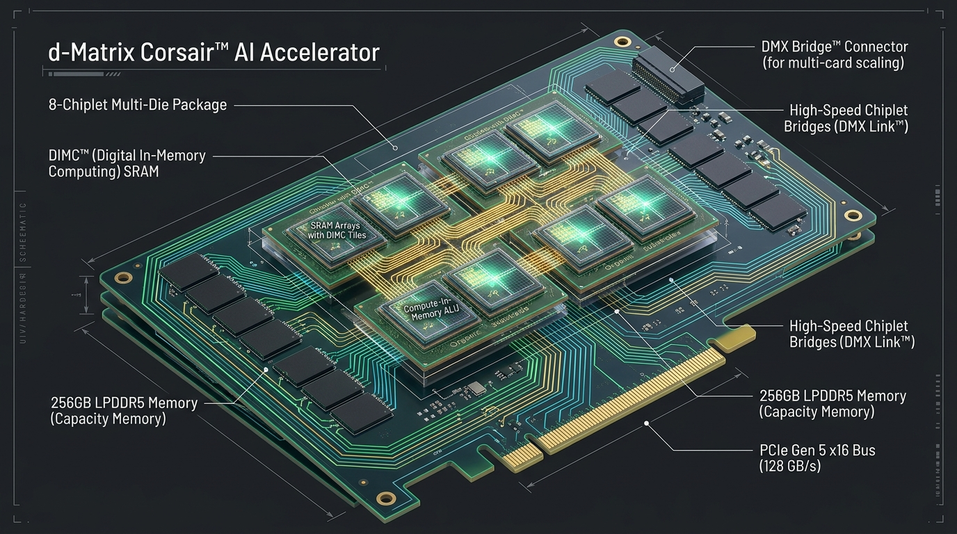
d-Matrix Corsair Architectural Blueprint:
+------------------------------------------------------------------------------------+
| d-MATRIX CORSAIR ACCELERATOR (Dual-SiP FHFL PCIe Gen 5 Card, ~300W TDP)            |
+------------------------------------------------------------------------------------+
|                                                                                    |
|  +-------------------------------------+  +-------------------------------------+  |
|  | SYSTEM-IN-PACKAGE 0 (SiP 0)         |  | SYSTEM-IN-PACKAGE 1 (SiP 1)         |  |
|  | - 4x TSMC Advanced Compute Chiplets |  | - 4x TSMC Advanced Compute Chiplets |  |
|  | - 1 GB High-Density DIMC SRAM       |  | - 1 GB High-Density DIMC SRAM       |  |
|  | - 75 TB/s Internal Memory Bandwidth |  | - 75 TB/s Internal Memory Bandwidth |  |
|  +-------------------------------------+  +-------------------------------------+  |
|                   ||                                         ||                    |
|  ================================================================================  |
|  DMX-Link Die-to-Die Interconnect Bridges (Ultra-Low Latency Cross-Chiplet Fabric) |
|  ================================================================================  |
|                   ||                                         ||                    |
|  +-------------------------------------+  +-------------------------------------+  |
|  | 256 GB LPDDR5 CAPACITY MEMORY (128 GB Per SiP, Cost-Effective Prompt Storage)   |  |
|  +---------------------------------------------------------------------------------+  |
|                                                                                    |
|  +------------------------------------------------------------------------------+  |
|  | PCIe GEN 5 x16 HOST INTERFACE & DMX BRIDGE MULTI-CARD EXPANSION INTERCONNECT  |  |
|  +------------------------------------------------------------------------------+  |
+------------------------------------------------------------------------------------+ 1. Digital vs. Analog In-Memory Computing
For decades, academic researchers explored Analog In-Memory Computing (AIMC) using memristors, phase-change memory (PCM), or flash memory arrays. In analog compute, input voltages are applied to memory rows, and matrix multiplication is performed using Ohm’s Law ($I = V \times G$) and Kirchhoff’s Current Law.
However, analog in-memory computing failed in commercial production due to critical flaws:
- Analog Noise and Drift: Analog circuits are extremely sensitive to temperature changes, thermal drift, and semiconductor manufacturing variations, causing numerical outputs to fluctuate unpredictably.
- ADC/DAC Conversion Bottlenecks: Converting digital activation tokens into analog voltages (via DACs) and converting analog currents back to digital numbers (via ADCs) consumes immense silicon area and power, negating the theoretical energy savings.
- Loss of Mathematical Precision: Analog circuits struggle to achieve more than 4 to 6 bits of effective precision, rendering them unsuitable for sensitive foundation models that collapse under quantization noise.
d-Matrix bypassed these obstacles by engineering Digital In-Memory Computing (DIMC):
- 100% Deterministic Digital Math: Corsair executes all arithmetic using standard digital logic gates (AND gates, adders, accumulators) embedded directly within custom SRAM bit-cell tiles.
- Zero Conversion Overhead: Inputs and outputs remain purely digital throughout the entire datapath, eliminating analog-to-digital converters entirely.
- Exact Bit-Level Reproducibility: Mathematical calculations are fully deterministic, matching standard IEEE floating-point and block-floating point specifications with zero drift.
2. 2 GB of SRAM at 150 TB/s Bandwidth
The physical memory density of Corsair represents a radical departure from traditional accelerator boards:
- 2 GB of On-Chip SRAM: A full-height, full-length (FHFL) Corsair PCIe card integrates two System-in-Package (SiP) modules containing eight chiplets, packing an unprecedented 2 Gigabytes of high-density on-chip SRAM (256 MB per chiplet).
- 150 TB/s Internal Memory Bandwidth: Because compute logic resides directly adjacent to the SRAM storage cells, the internal aggregate memory bandwidth reaches 150 Terabytes per second per card—nearly 20x the memory bandwidth of NVIDIA Blackwell (8 TB/s) and 45x that of Hopper H100 (3.35 TB/s).
- Massive Energy Efficiency: By keeping model weights stationary inside the SRAM cells and eliminating high-capacitance interposer wire transfers, Corsair slashes energy consumption per token by up to 20x compared to GPUs.
3. Tiered Memory Hierarchy: 2 GB SRAM + 256 GB LPDDR5
Unlike pure-SRAM chips (such as the Groq LPU) that lack external DRAM entirely and cannot hold large context buffers, Corsair features an intelligent two-tier memory architecture:
- Tier 1 (SRAM Compute Fabric - 2 GB, 150 TB/s): Stores active model weights and executes high-speed matrix-vector decoding.
- Tier 2 (Capacity Memory - 256 GB LPDDR5): Provides 256 GB of cost-effective capacity memory per card, used for prompt caching, KV cache storage for extended contexts, and staging model weights.
- This hybrid structure allows an enterprise server with multiple Corsair cards to host dense models up to 30 billion parameters resident in SRAM, while paging larger models or historical KV states from LPDDR5 without crashing.
Deep Dive: Corsair Chiplet Microarchitecture & Block Floating Point
To understand how d-Matrix Corsair achieves its execution throughput, we examine the microarchitecture of the DIMC computing tile, chiplet interconnects, and numerical representation.
1. The DIMC Computing Tile and Core Topology
Each of the eight chiplets on a Corsair accelerator contains an array of specialized DIMC Processing Tiles:
Detailed Microarchitecture of a d-Matrix DIMC Processing Tile:
+------------------------------------------------------------------------------------+
| d-MATRIX DIMC PROCESSING TILE SCHEMATIC                                            |
+------------------------------------------------------------------------------------+
|                                                                                    |
|   +----------------------------------------------------------------------------+   |
|   | ACTIVATION BROADCAST SHIFT REGISTERS (Input Vector Streaming)              |   |
|   +----------------------------------------------------------------------------+   |
|         |                     |                     |                     |        |
|         v                     v                     v                     v        |
|   +-----------+         +-----------+         +-----------+         +-----------+  |
|   | SRAM Cell |         | SRAM Cell |         | SRAM Cell |         | SRAM Cell |  |
|   | (Weight)  |         | (Weight)  |         | (Weight)  |         | (Weight)  |  |
|   |     +     |         |     +     |         |     +     |         |     +     |  |
|   | Digital   |         | Digital   |         | Digital   |         | Digital   |  |
|   | Logic MAC |         | Logic MAC |         | Logic MAC |         | Logic MAC |  |
|   +-----------+         +-----------+         +-----------+         +-----------+  |
|         |                     |                     |                     |        |
|         +---------------------+---------------------+---------------------+        |
|                                       v                                            |
|   +----------------------------------------------------------------------------+   |
|   | DIGITAL ACCUMULATION TREE & BLOCK EXPONENT SCALING LOGIC                   |   |
|   +----------------------------------------------------------------------------+   |
|                                       v                                            |
|   +----------------------------------------------------------------------------+   |
|   | TILE RESULT SCRATCHPAD & INTERCONNECT NETWORK INTERFACE                    |   |
|   +----------------------------------------------------------------------------+   |
|                                                                                    |
+------------------------------------------------------------------------------------+ - Weight-Stationary Bit-Cell Storage: Model weights are loaded once into the static 6T/8T SRAM bit-cells. Once loaded, weights never move across memory buses during token generation.
- In-Situ Digital MAC Arrays: Standard arithmetic logic is physically intertwined with the memory wordlines and bitlines. When an activation vector is broadcast across the tile, the multiplication and partial accumulation occur directly at the memory column boundaries.
- Digital Accumulator Trees: Multi-operand digital adder trees sum partial products across columns, feeding results into local scratchpad registers.
- Local Control Engine: A lightweight embedded RISC microcontroller inside each tile coordinates tensor tiling, buffer synchronization, and asynchronous data streaming.
2. Block Floating Point (BFP) Numerics
Floating-point multipliers consume substantial silicon area and electrical energy. To maximize compute density while maintaining model accuracy, Corsair relies on Block Floating Point (BFP) arithmetic:
- The Structure of BFP: A tensor tile (e.g., a 16-element or 32-element vector block) shares a single common 8-bit exponent, while each individual element is represented by a compact low-bit mantissa (BFP16, BFP8, or BFP4).
- Simplified Hardware Logic: Because exponents are shared across the block, the in-memory arithmetic units require only integer adders and multipliers, slashing circuit area and power consumption by over 70% compared to IEEE floating-point units.
- Lossless Inference Accuracy: Unlike aggressive post-training integer quantization (INT4) that suffers from activation outlier degradation, Block Floating Point dynamically tracks dynamic range at the fine-grained block level, preserving full BF16 baseline reasoning accuracy across LLMs.
$$ \mathbf{X} = 2^{E_{\text{shared}}} \times \left[ m_1, m_2, \dots, m_k ight], \quad m_i \in [-2^{p-1}, 2^{p-1}-1] $$
4. Circuit-Level Implementation: 8T SRAM Cells and Digital Adders
The fundamental breakthrough enabling Digital In-Memory Computing lies at the physical transistor and cell-layout level:
- 8T SRAM Cell Stability: Standard 6-transistor (6T) SRAM cells share read and write bitlines, making them vulnerable to read-disturb noise when multiple rows are activated simultaneously. d-Matrix implements an 8-transistor (8T) dual-port SRAM architecture, isolating the read port from the internal storage nodes. This allows activations to stream across read wordlines continuously without risking cell data corruption.
- Pitch-Matched Digital Logic: Rather than routing signals off the memory macro to distant arithmetic logic units, digital full adders and multiplication gates are physically pitch-matched to the memory column layout. Arithmetic takes place directly at the bitline sense amplifiers.
- Dynamic Range Preservation: The digital accumulator tree within each tile maintains 24-bit integer accumulators. This wide accumulation precision guarantees that long vector dot products (such as a 4,096-dimensional hidden vector multiplication) never suffer from accumulator overflow or round-off quantization errors.
3. Chiplet Packaging and the DMX-Link Interconnect
To scale the architecture across an accelerator card without suffering from inter-die communication bottlenecks, d-Matrix utilizes modular chiplets:
- DMX-Link Die-to-Die Interconnect: An ultra-low-latency, high-density physical interface connecting the 4 chiplets within each System-in-Package (SiP). DMX-Link provides multiple terabits per second of cross-chiplet bandwidth with under 5 nanoseconds of latency.
- DMX-Bridge Optical/Copper Scaling: An external edge connector on the Corsair card bracket allows direct card-to-card bridging, enabling multiple Corsair cards in a server chassis to communicate over a unified low-latency fabric without saturating host PCIe switches.
Software Ecosystem & Model Deployment with the Aviator Suite
Hardware without accessible compiler infrastructure cannot succeed in modern production. d-Matrix developed the Aviator Software Suite, an automated compiler, runtime, and deployment platform designed to run open-source models out of the box.
The d-Matrix Aviator Software Hierarchy:
+-----------------------------------------------------------------------------------+
| FRAMEWORK LAYER: PyTorch, Hugging Face Transformers, vLLM, ONNX Runtime           |
+-----------------------------------------------------------------------------------+
                                         |
+-----------------------------------------------------------------------------------+
| AVIATOR GRAPH COMPILER: Automatic Graph Ingestion & Block Quantization            |
| - Auto-partitions models between 2 GB SRAM (Compute) and 256 GB LPDDR5 (Cache)   |
| - Fuses multi-head attention, RoPE positional encoding, and RMSNorm operators     |
+-----------------------------------------------------------------------------------+
                                         |
+-----------------------------------------------------------------------------------+
| DIMC RUNTIME ENGINE & KERNEL SCHEDULER: Asynchronous Hardware Orchestration       |
| - Manages DMX-Link transfers, DMA double-buffering, and weight-stationary caching |
+-----------------------------------------------------------------------------------+
                                         |
+-----------------------------------------------------------------------------------+
| PHYSICAL HARDWARE: d-Matrix Corsair PCIe Cards (8-Chiplet DIMC Fabric)            |
+-----------------------------------------------------------------------------------+ 1. Model Compilation and Serving via Aviator
Deploying an open-weights foundation model (such as LLaMA-3.1-8B) on d-Matrix Corsair requires only a few lines of Python using the Aviator SDK:
# ============================================================================
# File: serve_corsair_llama.py
# Description: Serving LLaMA-3.1 on d-Matrix Corsair with Aviator & DIMC
# ============================================================================

import torch
import aviator
from aviator import AviatorEngine, QuantizationConfig

def deploy_model_on_corsair():
    print("Initializing d-Matrix Corsair DIMC Hardware Acceleration...")

    # 1. Configure Block Floating Point (BFP8) Quantization
    quant_cfg = QuantizationConfig(
        format="BFP8",
        block_size=32,
        preserve_accuracy=True
    )

    # 2. Ingest and Compile Model for 8-Chiplet SRAM Topology
    # Aviator automatically tiles weights to fit resident in 2GB on-chip SRAM
    print("Compiling model graph via Aviator Compiler...")
    engine = AviatorEngine.from_pretrained(
        model_name="meta-llama/Llama-3.1-8B-Instruct",
        quantization=quant_cfg,
        device="corsair:0",
        optimization_level=3
    )

    # 3. Initialize High-Performance Inference Context
    prompt = "Explain how digital in-memory computing breaks the memory wall."
    print(f"Prompt: {prompt}")

    # 4. Execute Low-Latency Autoregressive Generation
    # Generates tokens at >200 tok/s at Batch Size 1 with sub-10ms TTFT
    response = engine.generate(
        prompt=prompt,
        max_new_tokens=256,
        temperature=0.7,
        top_p=0.9
    )

    print("
Generated Output from Corsair Hardware:")
    print(response.text)
    print(f"
Execution Telemetry: Latency per token: {response.inter_token_latency_ms:.2f} ms")

if __name__ == "__main__":
deploy_model_on_corsair() 3. Speculative Decoding Acceleration with Corsair as Draft Engine
One of the most powerful production deployment architectures for d-Matrix Corsair is serving as a dedicated Speculative Decoding Draft Engine:
- The Asymmetric Speculative Paradigm: In speculative decoding, a smaller draft model (e.g., LLaMA-3.1-8B) proposes candidate token trees, which a massive target model (e.g., LLaMA-3.1-70B or 405B) verifies in parallel. The overall system speedup is strictly capped by the draft model’s generation latency.
- Sub-5ms Drafting Latency: Because the 8B draft model resides completely inside Corsair’s 2 GB of SRAM at 150 TB/s bandwidth, Corsair generates draft tokens at over 250 to 300 tokens per second per stream.
- Hybrid Datacenter Infrastructure: Enterprises pair Corsair PCIe cards with standard GPU servers. Corsair acts as the lightning-fast drafting co-processor, offloading repetitive draft loops and multiplying end-to-end GPU serving throughput by 2.5x to 3.5x while slashing overall datacenter power consumption.
2. High-Throughput Micro-Batched Serving with vLLM
d-Matrix integrates natively with vLLM, allowing enterprises to serve conversational endpoints using OpenAI-compatible APIs while harnessing Corsair’s 150 TB/s SRAM bandwidth:
# ============================================================================
# Script: launch_corsair_vllm.sh
# Description: Launch vLLM OpenAI API Server backed by d-Matrix Corsair DIMC
# ============================================================================

# Install Aviator Runtime and vLLM d-Matrix Plugin
pip install aviator-runtime vllm-dmatrix

# Configure Environment Variables for Corsair Hardware
export DMATRIX_DEVICE_IDS=0
export AVIATOR_NUM_THREADS=16
export AVIATOR_MEM_TIER_POLICY=AUTO_SPILL_LPDDR5

# Launch vLLM Service Hosting LLaMA-3.1-8B at Batch Size 1-16
python3 -m vllm.entrypoints.openai.api_server --model meta-llama/Llama-3.1-8B-Instruct --host 0.0.0.0 --port 8000 --device dmatrix --max-model-len 8192 --dtype bfp8 --block-size 16 --enforce-eager Architectural Comparison: d-Matrix Corsair vs. Groq LPU vs. NVIDIA H100
To provide infrastructure architects with objective guidance on inference accelerator selection, we evaluate d-Matrix Corsair against its closest competitors:
+----------------------------------------------------------------------------------------------------+
| GENERATIVE AI INFERENCE ACCELERATOR COMPARATIVE SPECS                                              |
+----------------------------------------------------------------------------------------------------+
| Architecture Metric           | NVIDIA H100 SXM5       | Groq LPU (GroqCard)  | d-Matrix Corsair           |
+-------------------------------+------------------------+----------------------+----------------------------+
| Core Architectural Paradigm   | SIMT GPU + TensorCores | Deterministic TSP    | Digital In-Memory (DIMC)   |
| Primary Silicon Packaging     | Monolithic + 2.5D CoWoS| Monolithic 14nm      | Dual-SiP 8-Chiplet Design  |
| On-Chip High-Speed SRAM       | 50 MB L2 Cache         | 230 MB Global SRAM   | 2,048 MB (2 GB) DIMC SRAM  |
| External Memory Subsystem     | 80 GB HBM3 (3.35 TB/s) | None (Zero DRAM)     | 256 GB LPDDR5 (Capacity)   |
| Peak Internal Memory Bandwidth| 3.35 TB/s (HBM3)       | 80 TB/s (SRAM)       | 150 TB/s (SRAM Fabric)     |
| Numerical Precision Formats   | FP8, FP16, BF16, TF32  | FP16, INT8, INT4     | BFP16, BFP8, BFP4, INT8/4  |
| Total Board Power (TDP)       | 700 W (High Thermal)   | ~185 W               | ~300 W (Standard PCIe)     |
| Small-Batch Latency (B=1)     | Moderate (Memory-Bound)| Blazing (SRAM-Bound) | Blazing (DIMC Zero-Shuttle)|
| Memory Spillover Support      | Yes (Native HBM)       | No (Hard Capacity OOM| Yes (Tiered LPDDR5 Pool)   |
+----------------------------------------------------------------------------------------------------+ 1. Key Architectural Takeaways
2. Corsair vs. NVIDIA Hopper H100
- Data Shuttling vs. In-Situ Compute: While the H100 must shuttle model weights across HBM3 physical buses for every generated token (burning power and hitting memory bandwidth ceilings), Corsair keeps weights stationary inside 2 GB of SRAM, executing math directly in-memory at 150 TB/s internal bandwidth.
- Power Efficiency at Low Latency: At low batch sizes ($B = 1\text{ to }4$), Corsair achieves up to 10x lower latency and 20x better energy efficiency while consuming only 300 W compared to the H100’s 700 W.
- Form Factor Flexibility: Corsair operates as a standard PCIe Gen 5 add-in board that plugs into existing enterprise 2U servers without requiring specialized liquid cooling infrastructure.
3. Corsair vs. Groq LPU
- SRAM Capacity Dominance: While Groq’s LPU provides exceptional deterministic latency, each Groq card contains only 230 MB of SRAM and zero external memory. Holding an 8B model requires clustering 8 to 16 Groq cards together. A single Corsair card packs 2 GB of SRAM (nearly 9x the SRAM of Groq), allowing an 8B model to fit resident on a single accelerator board.
- Tiered Capacity Memory: Groq has no DRAM fallback; if a model’s KV cache exceeds SRAM, generation fails. Corsair integrates 256 GB of LPDDR5 memory, providing a safe capacity tier for long-context prompt caching and KV cache spillover.
Production Deployment & Enterprise Scaling
Deploying d-Matrix Corsair in production enterprise environments requires understanding server chassis integration, multi-card topologies, and system telemetry monitoring.
1. Server Form Factors and Multi-Card Topologies
Corsair is designed for standard datacenter deployment across standard PCIe servers:
- Enterprise 2U/4U Server Nodes (4x to 8x Corsair Cards):
- An 8-card Corsair server pools 16 GB of ultra-dense DIMC SRAM (delivering over 1.2 Petabytes per second of aggregate internal memory bandwidth) and 2 Terabytes of LPDDR5 memory.
- Handles models from 8B to 70B parameters with exceptional throughput, serving thousands of concurrent interactive requests at sub-20ms latency.
- DMX-Bridge Multi-Card Expansion: Up to 4 adjacent Corsair cards can be linked via direct top-edge DMX-Bridge connectors, enabling unified tensor sharding without routing inter-card communications through the host CPU’s PCIe root complex.
Enterprise Server Node Architecture (8x d-Matrix Corsair Cards):
┌────────────────────────────────────────────────────────────────────────┐
│ STANDARD 4U ENTERPRISE SERVER NODE (8x CORSAIR PCIe ACCELERATORS)      │
│                                                                        │
│   [Card 0] <=== DMX-Bridge ===> [Card 1] <=== DMX-Bridge ===> [Card 2] │
│      ||                             ||                             ||  │
│   PCIe Gen 5 x16                 PCIe Gen 5 x16                 PCIe   │
│      ||                             ||                             ||  │
│   ==================================================================   │
│   Dual-Socket Host Processor (AMD EPYC / Intel Xeon 6)                 │
│   ==================================================================   │
│                                                                        │
│   AGGREGATE SPECIFICATIONS:                                            │
│   - 16 GB Ultra-Dense DIMC SRAM (1.2 PB/s Aggregate Memory Bandwidth)  │
│   - 2 TB Pooled LPDDR5 Capacity Memory for Extended Contexts           │
│   - ~2.4 kW Total Server Power Envelope (Standard Air-Cooled Datacenter│
└────────────────────────────────────────────────────────────────────────┘ 2. Telemetry and Health Monitoring with dmx-smi
System administrators monitor Corsair cards using the d-Matrix System Management Interface (dmx-smi):
- Query live accelerator telemetry:
# Check SRAM utilization, LPDDR5 memory allocations, and thermals dmx-smi --query-gpu=index,name,utilization.dimc,memory.sram.used,temperature.gpu --format=csv - Prometheus exporters track:
- DIMC Compute Saturation: Verify that in-memory arithmetic arrays operate at high duty cycles during generation.
- SRAM vs. LPDDR5 Paging Frequency: Ensure active model layers remain locked inside on-chip SRAM to prevent memory spillover slowdowns.
- Thermal Dissipation: Maintain operating die temperatures below safe thermal thresholds ($T_j \< 85^\circ\text{C}$) under continuous serving loads.
3. Summary and Strategic Roadmap
The d-Matrix Corsair platform marks a fundamental breakthrough in generative AI hardware. By replacing the data-shuttling von Neumann model with Digital In-Memory Computing, pairing 2 GB of on-chip SRAM at 150 TB/s with 256 GB of LPDDR5, and packaging the architecture in an energy-efficient 300W PCIe form factor, d-Matrix has broken the generative AI memory wall.
For enterprise teams seeking to deploy real-time AI copilots, interactive voice assistants, and high-concurrency LLM inference without paying astronomical GPU cloud bills, d-Matrix Corsair provides the speed, energy efficiency, and mathematical precision required to power the future of interactive intelligence.