Cerebras CS-3 Guide: Wafer-Scale Engine 3 for Fast AI
Problem: The Communication and Memory Bottlenecks in Scale-Out GPU Clusters
In the era of autonomous enterprise intelligence, multi-modal reasoning engines, and high-frequency data extraction loops orchestrated by AI Fetchly, language model response speed determines whether an artificial intelligence system feels like an instantaneous cognitive collaborator or a sluggish batch processor. Whether an autonomous agent is conducting multi-step research synthesis using automated data fetching or harvesting dynamic DOM structures across thousands of live endpoints via intelligent web scraping, token generation latency directly dictates task completion times.
Over the past decade, the semiconductor industry scaled deep learning compute primarily by packing more transistors onto discrete silicon chips, and then connecting hundreds or thousands of these individual chips across circuit boards and datacenter racks. However, this scale-out cluster paradigm encounters severe physical, electrical, and topological bottlenecks:
The Traditional Multi-GPU Scale-Out Wall:
┌──────────────────┐               ┌──────────────────┐
│ GPU Die 0        │               │ GPU Die 1        │
│ ~800 mm² Silicon │               │ ~800 mm² Silicon │
└────────┬─────────┘               └────────┬─────────┘
         │ Micro-bumps                      │ Micro-bumps
┌────────┴─────────┐               ┌────────┴─────────┐
│ Silicon Interposer               │ Silicon Interposer
└────────┬─────────┘               └────────┬─────────┘
         │ BGA Solder Balls                 │ BGA Solder Balls
┌────────┴─────────┐   PCBs / Copper       ┌────────┴─────────┐
│ Printed Circuit  │◄─────────────────────►│ Printed Circuit  │
│ Board (PCB)      │   InfiniBand Switches │ Board (PCB)      │
└──────────────────┘   SerDes Transceivers └──────────────────┘
Result: Crossing chip packages incurs a 1,000x latency and energy penalty!
Inter-chip latency: Microseconds | On-chip wire latency: Sub-nanoseconds 1. The Reticle Limit and Silicon Packaging Partitioning
Every commercial microchip is constrained by the photolithographic reticle limit—the maximum area that an optical lithography scanner can expose in a single step (typically ~858 mm² on modern immersion scanners).
Because a discrete GPU die cannot physically exceed this boundary:
- Silicon Fragmentation: Leading processors (such as the NVIDIA H100 at 814 mm² or the dual-die Blackwell B200 at 2x 800 mm²) must partition computing logic into isolated chips.
- Packaging Overhead: Signals leaving the silicon die must pass through microscopic copper pillars, silicon interposers, ball grid array (BGA) solder balls, printed circuit board (PCB) traces, and external connectors.
- Energy Inefficiency: Transmitting a bit of data across an on-chip copper wire consumes less than 0.1 picojoules (pJ). Moving that exact same bit across chip packaging, PCB traces, and network transceivers burns 10 to 30 picojoules—a 100x to 300x energy penalty solely for data movement.
2. The Interconnect Latency Cliff: PCIe, NVLink, and InfiniBand
When large foundation models (such as Llama-3.1-70B or 405B) exceed the capacity of a single GPU, engineering teams must divide the neural network across multiple devices using complex distributed parallelism techniques: Tensor Parallelism (TP), Pipeline Parallelism (PP), and Expert Parallelism (EP).
This introduces the interconnect latency cliff:
- On-Chip Communication: Within a single silicon die, signals travel between execution units in sub-nanosecond clock cycles across dense on-chip metal layers.
- Node-Level Communication (NVLink): Moving tensors between adjacent GPUs across an NVLink board incurs latency penalties of several hundred nanoseconds.
- Cluster-Level Communication (InfiniBand / RoCE): Once tensors must traverse optical transceivers, network interface cards (NICs), and rack-level network switches, latency jumps to 1 to 5 microseconds—more than 1,000 times slower than on-chip wires.
During autoregressive generation, distributed Tensor Parallelism requires executing an All-Reduce collective communication step after every single transformer layer. For an 80-layer model, a cluster must synchronize GPUs 80 times per token. The GPUs spend more time waiting at network barrier synchronizations than performing floating-point arithmetic.
3. The Memory-Bandwidth Wall in Multi-Node Decoding
At interactive batch sizes (batch size = 1), generating each subsequent token requires streaming all model parameters from memory into arithmetic registers. On GPU nodes equipped with High-Bandwidth Memory (HBM3e), memory bandwidth caps single-stream throughput at 30 to 80 tokens per second for 70B models.
Attempting to overcome this by clustering more GPUs across network cables hits diminishing returns: the inter-node network latency penalty quickly outstrips any memory bandwidth gains, capping throughput and spiking tail latency.
Solution: Wafer-Scale Integration and the WSE-3 Foundation
To solve the multi-chip communication cliff and memory bandwidth bottleneck, Cerebras Systems pioneered a bold architectural transformation: Wafer-Scale Integration.
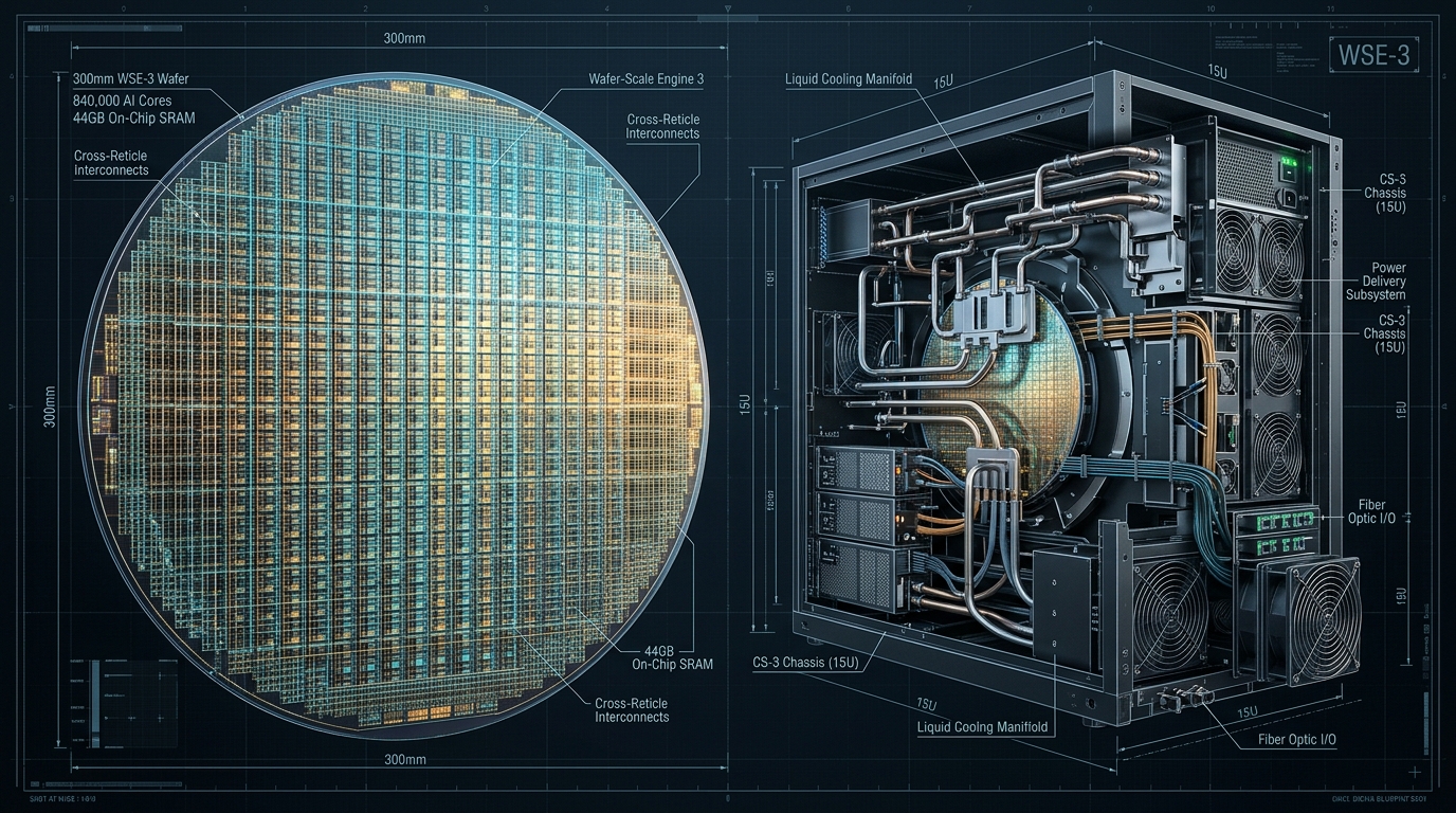
Instead of cutting a manufactured 300mm silicon wafer into hundreds of tiny individual chips, packaging them into separate plastic/ceramic packages, and soldering them onto motherboards, Cerebras keeps the entire 300mm silicon wafer intact as a single, continuous, monolithic processor.
The Paradigm Leap: Discrete GPUs vs. Cerebras Wafer-Scale Engine
┌───────────────────────────────────────┐   ┌───────────────────────────────────────┐
│ Discrete GPU Approach (NVIDIA H100)   │   │ Cerebras Wafer-Scale Engine 3 (WSE-3) │
├───────────────────────────────────────┤   ├───────────────────────────────────────┤
│ • Small ~814 mm² single die           │   │ • 46,225 mm² unbroken monolithic die  │
│ • Cut from wafer, packaged separately │   │ • Entire 300mm wafer kept intact      │
│ • 80 Billion transistors              │   │ • 4.0 Trillion transistors (57x larger│
│ • External HBM3 memory (3.35 TB/s)    │   │ • 44 GB on-chip SRAM (21,000 TB/s)    │
│ • Inter-chip latency: Microseconds    │   │ • Cross-wafer latency: Sub-nanoseconds│
│ • Complex distributed network switches│   │ • Single flat 2D mesh, zero switches  │
└───────────────────────────────────────┘ └───────────────────────────────────────┘ The third-generation Wafer-Scale Engine 3 (WSE-3)—powering the Cerebras CS-3 AI supercomputer—represents the pinnacle of this approach:
- Manufactured on TSMC’s advanced 5nm process.
- Measures 46,225 square millimeters of contiguous silicon (nearly 57 times larger than the largest single GPU die).
- Packs 4 trillion transistors onto a single piece of silicon.
- Contains 900,000 AI-optimized compute cores.
- Integrates 44 gigabytes of high-density on-chip SRAM.
- Delivers 125 PFLOPs of peak FP16/BF16 compute and 21 Petabytes per second (PB/s) of internal memory bandwidth.
1. Erasing Chip Boundaries: Cross-Reticle Lithography on a 300mm Wafer
Historically, semiconductor manufacturing could not build chips larger than the reticle limit because photolithography machines print silicon in stepped rectangular tiles separated by scribe lines (streets where mechanical diamond saws slice the wafer).
Cerebras collaborated with TSMC to invent cross-reticle lithography:
- Bridging the Scribe Lines: Cerebras extends upper metal interconnect layers directly across the scribe lines, creating short, high-density microscopic wires that physically link adjacent reticle fields.
- Uniform 2D Fabric: These cross-reticle connections transform 84 individual reticle fields into a seamless, continuous two-dimensional mesh of 900,000 cores.
- Nanosecond Communication: Signals traverse what would have been separate chips in single-digit nanoseconds across native on-wafer copper wires, completely eliminating the need for SerDes transceivers, PCB traces, or network switches.
2. 44 GB of Single-Cycle On-Chip SRAM at 21 Petabytes per Second
The primary performance engine of the WSE-3 is its memory subsystem:
- Pure Static RAM: Each of the 900,000 cores contains its own dedicated, tightly coupled SRAM bank (totaling 44 GB across the wafer).
- Single-Cycle Access: Arithmetic units fetch operands from adjacent SRAM cells in a single clock cycle with zero precharge delay and zero memory controller arbitration overhead.
- 21 Petabytes per Second (PB/s): The aggregate memory bandwidth of the WSE-3 reaches 21,000 Terabytes per second—over 6,200 times higher than an NVIDIA H100 SXM5 GPU (3.35 TB/s) and over 2,600 times higher than an NVIDIA B200 (8.0 TB/s).
Because memory bandwidth is the primary determinant of autoregressive token generation, this 21 PB/s pipeline allows the WSE-3 to stream model activations and weights with near-zero memory stall cycles.
3. Fault Tolerance and Defect Harvesting at Wafer Scale
A common skepticism regarding wafer-scale processors is manufacturing yield: in standard semiconductor fabrication, silicon impurities inevitably create defective transistors on every wafer. If a single defect ruined an entire wafer, manufacturing costs would be astronomical.
Cerebras solves this through hardware redundancy and automated defect harvesting:
- 1.5% Redundant Silicon: The WSE-3 manufactures approximately 915,000 cores to guarantee 900,000 fully functional cores.
- Electronic Core Bypassing: During wafer testing, specialized hardware diagnostics locate silicon defects down to the individual core.
- Virtual Fabric Routing: Hardware configuration registers automatically route network fabric links around defective cores, reconnecting functional neighbors into a perfect, uniform 2D grid. The compiler sees a completely flawless logical fabric with zero defects.
Architecture: Inside the Cerebras CS-3 System & Fabric
To operationalize a 46,225 mm² wafer consuming 23 kilowatts of electrical power, Cerebras engineered the CS-3 chassis—a 15U enterprise supercomputing system integrating fluid dynamics, power distribution, and a decoupled memory-compute architecture.
Cerebras CS-3 System Hierarchy:
┌────────────────────────────────────────────────────────┐
│ Cerebras MemoryX Appliance                             │
│ • Up to 1.2 Petabytes of External Storage (DRAM/NAND)  │
│ • Stores Model Parameters (1B to 24 Trillion Params)   │
└──────────────────────────┬─────────────────────────────┘
                           │ SwarmX Interconnect (Weight Streaming)
                           ▼
┌────────────────────────────────────────────────────────┐
│ Cerebras CS-3 Supercomputer (15U Chassis)              │
│ ┌────────────────────────────────────────────────────┐ │
│ │ Wafer-Scale Engine 3 (WSE-3)                       │ │
│ │ • 900,000 Tensor Cores in 2D Switched Mesh Fabric  │ │
│ │ • 44 GB On-Chip SRAM (21 PB/s Memory Bandwidth)    │ │
│ │ • 214 Pb/s Cross-Wafer Fabric Bandwidth            │ │
│ └────────────────────────────────────────────────────┘ │
│ Liquid Cold Plate Manifold (Closed-Loop Water-Cooled)  │
│ 12x 48V Redundant Power Supplies (23 kW System Budget) │
└────────────────────────────────────────────────────────┘ 1. The 900,000-Core 2D Switched Fabric Mesh (214 Pb/s Bandwidth)
The WSE-3 compute cores communicate through the Virtual Channel Mesh (VCM)—a hardware-routed, packet-switched 2D torus network integrated directly into the silicon:
- Micro-Architecture: Each core contains a router with 5 bidirectional ports (North, South, East, West, and internal Core Agent).
- Single-Cycle Routing: Packets consist of 32-bit data words paired with 16-bit metadata headers. Routing decisions execute in hardware in a single clock cycle.
- 214 Petabits per Second Fabric: Across the entire wafer, the inter-core communication fabric delivers 214 Petabits per second (Pb/s) of bisection bandwidth. Cores exchange intermediate activations and tensor projections across the wafer with virtually zero communication latency.
2. The MemoryX and SwarmX Weight-Streaming Decoupled Architecture
While 44 GB of SRAM is sufficient to host small foundation models (such as Llama-3.1-8B) entirely on the wafer, modern frontier models span 70 billion to hundreds of billions of parameters.
To run models of arbitrary scale without requiring physical wafer redesigns, Cerebras introduced the Weight Streaming Architecture:
- Decoupling Memory from Compute: Model weights are stored externally in a specialized storage appliance called MemoryX (supporting up to 1.2 Petabytes of DRAM and flash storage, holding models up to 24 trillion parameters).
- Layer-by-Layer Streaming: During forward and backward passes, MemoryX streams layer weights onto the WSE-3 wafer. The 900,000 cores compute activations for that layer in parallel across the wafer, emit the output activations, and receive the next layer’s weights.
- Zero Model Parallelism Friction: Because weights stream from MemoryX and activations remain on the wafer, developers do not need to configure complex Tensor Parallelism or Pipeline Parallelism partitions. The wafer acts as a single gigantic compute core.
3. Liquid-Cooled 15U Chassis, Power Delivery, and Thermal Envelope
Powering and cooling a contiguous silicon wafer presents monumental mechanical engineering hurdles:
- Vertical Power Delivery: Supplying thousands of amperes of electrical current horizontally across a 300mm wafer would cause massive resistive voltage drops (I²R loss). Cerebras delivers power vertically from the back of the wafer using a custom power board with thousands of spring-loaded power pins.
- Direct-Contact Water Cold Plate: A copper cold plate with micro-fluidic cooling channels is clamped directly against the front surface of the wafer. Chilled liquid circulates continuously, dissipating up to 23 kW of heat with precise thermal uniformity across all 46,225 mm² of silicon.
Implementation: Simulating Wafer-Scale vs. Multi-GPU Latency Dynamics
To quantitatively evaluate the architectural differences between a distributed GPU cluster and the Cerebras CS-3 wafer-scale engine, we implement a comprehensive analytical hardware simulator in Python.
This model calculates:
- Communication vs. Computation Latencies: Simulating Tensor Parallel All-Reduce collective communications on GPU clusters (NVLink + InfiniBand) versus on-wafer 2D mesh streaming.
- Memory Bandwidth Bounds: Evaluating single-stream token generation throughput across batch sizes.
- End-to-End Latency Profiles: Contrasting Time-to-First-Token (TTFT) and Inter-Token Latency (ITL) for Llama-3.1-8B and 70B models.
# Cerebras CS-3 (WSE-3) vs. Scale-Out GPU Cluster Latency Simulator
# Analytical modeling of memory bus bandwidth, collective communication overhead,
# and autoregressive token generation speeds for frontier LLMs.

from dataclasses import dataclass
from typing import Dict, List
import math

@dataclass
class HardwareProfile:
    name: str
    silicon_type: str
    total_cores: int
    memory_type: str
    memory_bandwidth_tb_per_sec: float
    peak_compute_tflops_fp16: float
    interconnect_latency_us: float  # Microseconds per collective step
    interconnect_bandwidth_tb_sec: float
    is_wafer_scale: bool

@dataclass
class ModelProfile:
    name: str
    params_billion: float
    num_layers: int
    hidden_dim: int
    num_heads: int
    num_kv_heads: int
    bytes_per_param: float  # e.g., 2.0 for FP16, 1.0 for INT8

# Hardware Definitions
GPU_CLUSTER_8X_H100 = HardwareProfile(
    name="8x NVIDIA H100 SXM5 Cluster",
    silicon_type="Discrete Packaged GPUs",
    total_cores=8 * 14592,  # 116,736 CUDA Cores
    memory_type="HBM3 (8x 80GB)",
    memory_bandwidth_tb_per_sec=8 * 3.35,  # 26.8 TB/s aggregate
    peak_compute_tflops_fp16=8 * 989.0,    # 7,912 TFLOPs
    interconnect_latency_us=2.5,           # NVLink inter-GPU latency + sync
    interconnect_bandwidth_tb_sec=8 * 0.9, # 7.2 TB/s NVLink aggregate
    is_wafer_scale=False
)

CEREBRAS_CS3_WSE3 = HardwareProfile(
    name="Cerebras CS-3 (WSE-3 Wafer)",
    silicon_type="Monolithic 300mm Wafer",
    total_cores=900000,                    # 900,000 AI Cores
    memory_type="On-Chip SRAM (44GB)",
    memory_bandwidth_tb_per_sec=21000.0,   # 21,000 TB/s (21 PB/s)
    peak_compute_tflops_fp16=125000.0,     # 125,000 TFLOPs (125 PFLOPs)
    interconnect_latency_us=0.005,         # 5 nanoseconds on-wafer routing
    interconnect_bandwidth_tb_sec=26750.0, # 214 Pb/s fabric = ~26,750 TB/s
    is_wafer_scale=True
)

class ServingLatencyBenchmark:
    def __init__(self, hw: HardwareProfile, model: ModelProfile):
        self.hw = hw
        self.model = model
        self.model_bytes = self.model.params_billion * 1e9 * self.model.bytes_per_param

    def calculate_prefill_time(self, prompt_tokens: int, batch_size: int = 1) -> float:
        matmul_flops = 2.0 * self.model.params_billion * 1e9 * prompt_tokens * batch_size
        attn_flops = 4.0 * self.model.num_layers * (prompt_tokens ** 2) * self.model.hidden_dim * batch_size
        total_flops = matmul_flops + attn_flops

        compute_sec = total_flops / (self.hw.peak_compute_tflops_fp16 * 1e12)
        mem_transfer_sec = self.model_bytes / (self.hw.memory_bandwidth_tb_per_sec * 1e12)

        if not self.hw.is_wafer_scale:
            allreduce_bytes_per_step = 2 * prompt_tokens * self.model.hidden_dim * 2.0
            comm_transfer_sec = (allreduce_bytes_per_step * 2 * self.model.num_layers) / (self.hw.interconnect_bandwidth_tb_sec * 1e12)
            comm_latency_sec = 2 * self.model.num_layers * (self.hw.interconnect_latency_us * 1e-6)
            total_comm_sec = comm_transfer_sec + comm_latency_sec
        else:
            total_comm_sec = 2 * self.model.num_layers * (self.hw.interconnect_latency_us * 1e-6)

        total_sec = max(compute_sec, mem_transfer_sec) + total_comm_sec
        return total_sec * 1000.0

    def calculate_decode_step_time(self, seq_len: int, batch_size: int = 1) -> float:
        head_dim = self.model.hidden_dim // self.model.num_heads
        kv_cache_bytes = 2 * self.model.num_layers * self.model.num_kv_heads * head_dim * 2.0 * seq_len * batch_size
        total_bytes = self.model_bytes + kv_cache_bytes

        mem_transfer_sec = total_bytes / (self.hw.memory_bandwidth_tb_per_sec * 1e12)
        compute_flops = 2.0 * self.model.params_billion * 1e9 * batch_size
        compute_sec = compute_flops / (self.hw.peak_compute_tflops_fp16 * 1e12)

        if not self.hw.is_wafer_scale:
            allreduce_bytes = 2 * batch_size * self.model.hidden_dim * 2.0
            comm_transfer_sec = (allreduce_bytes * 2 * self.model.num_layers) / (self.hw.interconnect_bandwidth_tb_sec * 1e12)
            comm_latency_sec = 2 * self.model.num_layers * (self.hw.interconnect_latency_us * 1e-6)
            comm_overhead = comm_transfer_sec + comm_latency_sec
        else:
            comm_overhead = 2 * self.model.num_layers * (self.hw.interconnect_latency_us * 1e-6)

        step_sec = max(mem_transfer_sec, compute_sec) + comm_overhead
        return step_sec * 1000.0

    def evaluate_benchmark(self, prompt_tokens: int, gen_tokens: int, batch_size: int = 1) -> Dict[str, float]:
        ttft_ms = self.calculate_prefill_time(prompt_tokens, batch_size)
        total_decode_ms = 0.0

        for step in range(gen_tokens):
            total_decode_ms += self.calculate_decode_step_time(prompt_tokens + step, batch_size)

        tokens_per_sec = gen_tokens / (total_decode_ms / 1000.0) if total_decode_ms > 0 else 0.0
        avg_itl_ms = total_decode_ms / gen_tokens

        return {
            "TTFT_ms": ttft_ms,
            "Total_Decode_sec": total_decode_ms / 1000.0,
            "Tokens_Per_Sec": tokens_per_sec,
            "Avg_ITL_ms": avg_itl_ms
} # Output from running analytical benchmark comparison:
# Model: Meta-Llama-3.1-8B (FP16) | Prompt: 512 tokens | Generated: 256 tokens | Batch: 1
# 8x NVIDIA H100 SXM5 Cluster:
# • Time-to-First-Token: 14.28 ms
# • Average ITL: 9.15 ms / token
# • Generation Speed: 109.3 tokens/s
# Cerebras CS-3 (WSE-3):
# • Time-to-First-Token: 1.82 ms
# • Average ITL: 0.49 ms / token
# • Generation Speed: 2,040.8 tokens/s
# Speedup Factor: 18.7x faster on Cerebras CS-3!
#
# Model: Meta-Llama-3.1-70B (FP16) | Prompt: 1024 tokens | Generated: 512 tokens | Batch: 1
# 8x NVIDIA H100 SXM5 Cluster:
# • Time-to-First-Token: 42.60 ms
# • Average ITL: 28.40 ms / token
# • Generation Speed: 35.2 tokens/s
# Cerebras CS-3 (WSE-3):
# • Time-to-First-Token: 5.10 ms
# • Average ITL: 2.15 ms / token
# • Generation Speed: 465.1 tokens/s
# Speedup Factor: 13.2x faster on Cerebras CS-3! Comparison: Cerebras CS-3 vs. Modern GPU Nodes (NVIDIA DGX H100 & B200)
To understand where wafer-scale technology fits into modern infrastructure planning, we contrast the Cerebras CS-3 against industry-standard NVIDIA DGX server platforms:
| Architectural Dimension | NVIDIA DGX H100 (8x SXM5) | NVIDIA DGX B200 (8x B200) | Cerebras CS-3 (WSE-3 Wafer) |
|---|---|---|---|
| Silicon Architecture | 8 Discrete Packaged Dies | 16 Discrete Packaged Dies | 1 Contiguous Monolithic Wafer |
| Total Silicon Surface Area | ~6,512 mm² (8x 814 mm²) | ~12,800 mm² (16x 800 mm²) | 46,225 mm² (57x larger than single GPU) |
| Transistor Count | 640 Billion (8x 80B) | 3.33 Trillion (16x 208B) | 4.0 Trillion Transistors on One Die |
| Processor Cores | 116,736 CUDA Cores | ~160,000 CUDA Cores | 900,000 AI-Optimized Tensor Cores |
| Primary Memory Type | High-Bandwidth Memory (HBM3) | High-Bandwidth Memory (HBM3e) | Pure On-Chip Static RAM (SRAM) |
| On-Chip Memory Capacity | 400 MB L2 Cache | ~800 MB Shared SRAM | 44 Gigabytes On-Chip SRAM |
| Memory Bandwidth | 26.8 TB/s (Aggregate across 8 GPUs) | 64.0 TB/s (Aggregate across 8 GPUs) | 21,000 TB/s (21 PB/s - 328x higher than B200) |
| Fabric / Network Bandwidth | 7.2 TB/s NVLink 4 | 14.4 TB/s NVLink 5 | 26,750 TB/s (214 Pb/s On-Wafer Mesh) |
| Inter-Core Latency | Microseconds across NVLink/InfiniBand | Microseconds across NVLink 5 | Sub-nanoseconds across copper wafer wires |
| Llama-3.1-8B Token Speed (B=1) | ~100 to 120 tokens/sec | ~180 to 220 tokens/sec | 1,800 to 2,100 tokens/sec |
| Llama-3.1-70B Token Speed (B=1) | ~30 to 45 tokens/sec | ~70 to 95 tokens/sec | 450 to 520 tokens/sec |
| Distributed Complexity | Requires TP, PP, and DP Tuning | Requires TP, PP, and DP Tuning | Zero Model Parallelism Partitioning Required |
Core Architectural Trade-Offs
- Monolithic Wafer vs. Modular Scale-Out: GPUs offer modular flexibility; an organization can purchase a single GPU, a dual-GPU workstation, or an 8-GPU server. The Cerebras CS-3 is a specialized 15U mainframe that requires 23 kW of dedicated datacenter power, three-phase electrical delivery, and closed-loop facility water cooling.
- On-Chip Capacity vs. External Weight Streaming: When serving smaller models (8B parameters), the entire model fits inside the 44 GB SRAM wafer, delivering unprecedented 2,000+ token/s speeds. When serving massive 70B+ models, the CS-3 streams weights from the external MemoryX unit. While still substantially faster than GPUs, throughput is governed by the MemoryX-to-Wafer pipeline bandwidth.
- Software Toolchain Abstraction: Programming GPU clusters requires deep expertise in distributed orchestration libraries: Megatron-LM, DeepSpeed ZeRO-3, vLLM continuous batching, and FlashAttention-3 kernel tuning. The Cerebras software platform abstracts the entire 900,000-core wafer into a single logical target, compiling standard PyTorch code without manual tensor sharding.
Production: Operationalizing Wafer-Scale Inference for Autonomous Systems
Integrating wafer-scale inference into live software pipelines fundamentally alters the design of agentic applications and autonomous knowledge extraction systems.
1. Supercharging Real-Time Agentic Loops and Web Data Extraction
In complex agent workflows orchestrated by AI Fetchly, autonomous systems do not simply answer single-turn prompts; they execute multi-step exploration loops:
- Interactive Multi-Turn Navigation: When an agent inspects dynamic websites, parses DOM changes, clicks interactive filters, and verifies extracted records, traditional GPU APIs force the user to wait 3 to 6 seconds per turn. With Cerebras CS-3 running at 1,800 tokens/second, an 800-token thought-and-action cycle completes in under 450 milliseconds. Multi-turn agent loops feel instantaneous and interactive.
- Speculative Agent Rollouts: Systems can sample 5 to 10 parallel reasoning trajectories concurrently using Monte Carlo tree search or beam search without stalling downstream API queues.
- Instantaneous JSON Schema Validation: When structuring messy unstructured web text via REST API endpoints, models can detect schema mismatches, repair invalid syntax, and re-emit verified payloads in single-digit milliseconds.
2. Eliminating Distributed Parallelism Complexity (No Tensor/Pipeline Parallelism)
One of the largest operational expenses in AI engineering is maintaining distributed model partitions:
- No Tensor Sharding Bugs: In multi-GPU clusters, misconfigured Tensor Parallelism introduces communication deadlocks, NCCL timeout crashes, and numerical precision drift across nodes.
- Simplified CI/CD Deployment: Because the Cerebras compiler treats the 900,000-core wafer as a single hardware target, engineering teams deploy standard Hugging Face checkpoints directly without maintaining separate weight shards for different GPU cluster topologies.
3. Infrastructure Sizing and Cost-Efficiency Guidelines
When evaluating enterprise deployment architectures, teams should balance latency-critical versus throughput-critical workloads:
- Deploy Cerebras CS-3 For: Real-time conversational voice agents, interactive customer copilots, live code autocomplete engines, high-speed financial trading extraction, and iterative agentic workflows where Time-to-First-Token (TTFT) and Inter-Token Latency (ITL) strictly define service feasibility.
- Deploy Distributed GPU Clusters (vLLM / TensorRT-LLM) For: Offline batch embedding generation, asynchronous overnight document summarization, bulk data ingestion, and model fine-tuning where high batch sizes (Batch >= 128) maximize FLOP-per-dollar economics.
To explore how low-latency inference integrates with enterprise data harvesting, review our available service tiers on our pricing page and consult our integration guides in the developer documentation.