Cadence Tensilica Guide: Neo NPU & Vision DSP Architecture
The Edge Vision Processing Dilemma: Bandwidth Starvation and the Custom Instruction Chasm
The exponential deployment of computer vision and on-device machine learning has transformed the embedded systems landscape. From automotive advanced driver-assistance systems (ADAS) and autonomous robotics to high-end mobile smartphones, surveillance cameras, and industrial automated optical inspection (AOI), embedded devices must evaluate complex neural networks in real time. Processing high-resolution visual feeds—such as multi-camera 4K HDR streams at 60 frames per second—demands trillions of mathematical operations every second under strict physical power and thermal envelopes.
However, attempting to execute modern vision workloads on conventional embedded processor architectures exposes four acute microarchitectural bottlenecks:
- The Von Neumann DRAM Energy Wall and Bandwidth Bottlenecks: In traditional embedded system-on-chip (SoC) architectures, host central processing units (CPUs) and graphics processing units (GPUs) are physically separated from dynamic RAM (LPDDR4/5) by macroscopic board traces and complex bus crossbars. Shuttling high-resolution image tensors, convolutional filter weights, and intermediate activation maps across external memory buses consumes between 70% and 90% of dynamic system energy. In battery-powered edge cameras or fanless automotive modules, this continuous memory traffic triggers rapid thermal throttling and exhausts power budgets within minutes.
- The Vector-Matrix Asymmetry in Vision Transformers (ViTs): While early embedded AI hardware was engineered exclusively around dense 2D convolutional layers, modern computer vision has rapidly converged on hybrid architectures and Vision Transformers (ViTs). Vision Transformers interleave dense matrix multiplications with complex vector operations: patch embeddings, multi-head self-attention projections, Softmax normalization distributions, LayerNorm/RMSNorm scalings, and Rotary Position Embeddings (RoPE). Standard hardwired neural processing units (NPUs) that lack wide, programmable vector execution engines experience severe pipeline stalls, forcing expensive fallback data transfers to host CPUs.
- The Proprietary Operator Lag and the Silicon Extensibility Gap: Deep learning research evolves at breakneck velocity, introducing novel activation functions (such as SwiGLU or dynamic GeLU), customized sparsity masks, and non-standard quantization representations (such as micro-scaling formats MXFP6/MXFP4). Fixed-function silicon IP blocks frozen in silicon masks cannot adapt to these algorithmic shifts. When an emerging model encounters an unsupported mathematical operator, the entire inference graph is fragmented, forcing high-latency CPU context switches that destroy real-time latency guarantees.
- Toolchain Fragmentation and Heterogeneous Deployment Friction: Silicon design teams building heterogeneous SoC product tiers—spanning from sub-watt wearable sensors to high-performance automotive cockpits—face prohibitive non-recurring engineering (NRE) costs if forced to maintain disparate programming environments for different computing engines. Developers require a unified, production-grade software development kit (SDK) that seamlessly partitions, quantizes, and compiles graphs across digital signal processors (DSPs), dedicated neural processing units (NPUs), and specialized neural co-processors under a single API.
Addressing these foundational challenges requires a modular, configurable processor IP architecture that unites dense systolic matrix acceleration with ultra-wide SIMD vector execution, backed by hardware-level instruction extensibility and automated graph compilation.
Introducing Cadence Tensilica Neo NPU and Vision Q8: Scalable Silicon IP
Cadence Design Systems—the global electronic design automation (EDA) and semiconductor IP leader—solved the embedded intelligence challenge with the Cadence Tensilica Neo NPU IP family and the 7th-generation Tensilica Vision Q8 DSP.
Representing one of the semiconductor industry’s most flexible, silicon-proven neural acceleration architectures, Cadence Tensilica IP has been deployed across billions of commercial silicon chips worldwide. Powered by the configurable Xtensa® processor architecture and the proprietary Tensilica Instruction Extension (TIE) language, the Tensilica AI platform spans from ultra-low-power, always-on IoT sensors to high-performance multi-camera automotive supercomputers.
+-------------------------------------------------------------------------+
|                  Cadence Tensilica AI Processor IP Portfolio            |
+-------------------------------------------------------------------------+
| Flagship DSP:       Tensilica Vision Q8 DSP (1024-bit SIMD Vector Engine|
| Peak DSP Compute:   3.84 TOPS INT8 | 129 GFLOPS FP32 per Single Core    |
| Dedicated NPU IP:   Cadence Neo NPU Family (Neo N10, N20, N40, N80 Cores|
| Scalable NPU TOPS:  8 GFLOPS up to 80 TOPS in a Single Core (Multi-Tile)|
| Numerical Formats:  INT4, INT8, INT16, FP16, BF16 (Per-Layer Mixed Mode)|
| Instruction Engine: Extensible Tensilica Instruction Extension (TIE)    |
| Memory Architecture:Tightly Coupled Memories (IRAM/DRAM) + AXI5 DMA     |
| Software Platform:  Cadence NeuroWeave™ SDK & Tensilica Vision SDK      |
+-------------------------------------------------------------------------+ Key microarchitectural breakthroughs integrated into the Cadence Tensilica AI platform include:
- 1024-bit SIMD Vector Architecture in Vision Q8: The 7th-generation flagship Tensilica Vision Q8 DSP features a massive 1024-bit wide Single Instruction Multiple Data (SIMD) execution pipeline, delivering up to 3.84 TOPS of INT8 compute and 129 GFLOPS of IEEE FP32 precision per core, doubling the vector throughput of previous architectures.
- Scalable Neo NPU Family (Up to 80 TOPS Single Core): The dedicated Neo NPU family scales from 256 MACs to 32,768 MACs per core, providing configurable compute profiles from 8 GFLOPS in ultra-low-power IoT nodes up to 80 TOPS in a single core (and hundreds of TOPS in multi-core clusters) for enterprise edge servers and automotive cockpits.
- Tensilica Instruction Extension (TIE) Customizability: Enables semiconductor architects to define proprietary hardware instructions, custom register files, and non-standard data types directly in silicon using the TIE language. Custom instructions synthesize automatically into execution datapaths and are natively recognized by the compiler without manual assembly rewrites.
- Native Transformer and Multimodal Acceleration: Purpose-built hardware execution blocks accelerate multi-head self-attention mechanisms, Softmax normalizations, dynamic layer scaling, and non-linear activation functions, delivering a 20-fold machine learning throughput increase over previous DSP generations.
- Unified NeuroWeave™ Software Development Kit: Provides a comprehensive, production-grade toolchain that automates post-training quantization (PTQ), structural pruning, operator fusion, and memory allocation across PyTorch, TensorFlow, ONNX, and Android NNAPI.
Enterprises deploying large-scale neural network training, automated data extraction, and multimodal reasoning clusters can connect their Cadence Tensilica edge silicon infrastructure with real-time data ingestion infrastructure to stream high-velocity datasets directly into tightly coupled local memory for immediate vectorized processing and continuous fine-tuning. By marrying configurable microarchitectural flexibility with industrial software maturity, Cadence Tensilica establishes the premier foundation for on-device physical AI and vision intelligence.
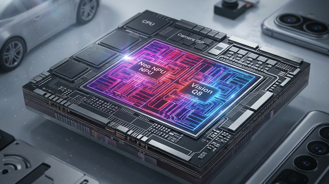
Architectural Deep Dive: Vision Q8 1024-Bit SIMD, Neo NPU Clusters, and TIE Extensibility
The exceptional computational density and energy efficiency of the Cadence Tensilica platform stem from its dual-engine microarchitecture: the ultra-wide vector capabilities of the Vision Q8 DSP, the high-density systolic matrix compute of the Neo NPU, and hardware-level instruction extensibility via TIE.
The Heterogeneous Vision & AI Tile Architecture
In contemporary edge vision SoCs, Cadence Tensilica IP is deployed either as a standalone high-performance vision DSP (Vision Q8), a dedicated neural accelerator (Neo NPU), or a tightly coupled heterogeneous compute complex:
+-----------------------------------------------------------------------------------+
|                  Cadence Tensilica Heterogeneous Vision & AI SoC                  |
+-----------------------------------------------------------------------------------+
|  +------------------------+  +-------------------------------------------------+  |
|  | AXI5 / OCP Host Bus    |  | Autonomous Multi-Channel Direct Memory Access   |  |
|  | High-Throughput Fabric |  | 128-bit / 256-bit Wide DMA Engine with 2D Tiling|  |
|  +-----------+------------+  +------------------------+------------------------+  |
|              |                                        |                           |
|  +-----------v----------------------------------------v------------------------+  |
|  |           Ultra-Low Latency Crossbar Switch & Inter-Core Fabric             |  |
|  +-----------------------------------------------------------------------------+  |
|        |                                        |                                 |
|  +-----v-------------------------------+  +-----v-------------------------------+ |
|  | Cadence Tensilica Vision Q8 DSP     |  | Cadence Neo NPU Core                | |
|  | - 32-bit Xtensa VLIW Controller    |  | - Hardware Graph Dispatch Sequencer | |
|  | - 1024-bit Wide SIMD Vector Unit   |  | - 2D Systolic Matrix Multiply Engine| |
|  | - 1,024 8-bit MACs per Clock Cycle |  | - 256 to 32,768 MACs (Up to 80 TOPS)| |
|  | - IEEE FP32 & FP16 Vector Floating |  | - Native Attention & Softmax Engine | |
|  | - Tightly Coupled IRAM/DRAM (512KB) |  | - Local Multi-Bank Scratchpad SRAM  | |
|  | - Custom TIE Application Extenders  |  | - Real-Time Lossless Decompression  | |
|  +-------------------------------------+  +-------------------------------------+ |
+-----------------------------------------------------------------------------------+ This decoupled architecture allocates tasks according to mathematical structure:
- Vision Q8 DSP (Classical Computer Vision & Vector Processing): Handles irregular, non-GEMM algorithms: image signal processing (ISP) post-processing, sensor fusion, spatial filtering, geometric warps, feature point extraction (FAST, ORB), optical flow, and transformer vector operations (RMSNorm, Softmax, RoPE).
- Neo NPU Core (Dense Matrix Tensor Contraction): Dedicated strictly to heavy 2D matrix-matrix multiplications (GEMM) and convolutions across INT4, INT8, INT16, and FP16 precisions. The Neo NPU executes matrix layers with maximum silicon area efficiency, passing activation outputs directly to the Vision Q8 or local memory buffers.
Tensilica Vision Q8 Microarchitecture: 1024-bit SIMD Power
The Tensilica Vision Q8 DSP represents a technological leap over traditional 512-bit DSP architectures. Its execution core is structured around a multi-issue Very Long Instruction Word (VLIW) instruction pipeline coupled with a 1024-bit SIMD vector datapath:
- 1,024 8-bit Multipliers: In a single clock cycle, the 1024-bit SIMD execution unit can perform 1,024 8-bit multiply-accumulate operations, 512 16-bit MACs, or 256 32-bit MACs.
- Dual-Issue Vector Execution: The VLIW architecture allows the processor to issue a 1024-bit vector arithmetic operation, a vector load, a vector store, and a scalar address update concurrently in every clock cycle, achieving near-100% vector ALU utilization.
- Native IEEE Floating-Point Support: Incorporates vector floating-point pipelines delivering 129 GFLOPS of IEEE single-precision (FP32) and over 500 GFLOPS of half-precision (FP16) compute, providing the numerical dynamic range necessary for high-precision robotic SLAM, depth estimation, and radar/lidar point cloud processing.
- Tightly Coupled Local Memory (TCM): Eliminates external memory latency by connecting the execution core directly to local Instruction RAM (IRAM) and Data RAM (DRAM). Operands are accessed with single-cycle latency without cache tag overhead or arbitration delays.
The Power of Tensilica Instruction Extension (TIE)
The definitive architectural differentiator of Cadence Tensilica processors is the Tensilica Instruction Extension (TIE) methodology. In conventional fixed-architecture processors (such as standard ARM or RISC-V cores), modifying execution pipelines requires multi-year silicon redesigns.
With TIE, semiconductor architects write high-level functional descriptions of custom execution units, state registers, and multi-cycle execution pipelines:
// conceptual_tie_example.tie
// Tensilica Instruction Extension defining custom fused activation instruction

operation FUSED_GELU_SCALE {out VReg1024 res, in VReg1024 act, in SReg32 scale} {
    // Custom hardware datapath synthesized directly into Vision Q8 execution stage
    // Performs polynomial approximation of GeLU activation scaled by dynamic factor
    wire [1023:0] gelu_out;
    // Hardware datapath logic mapped in standard cells
    assign res = gelu_out * scale;
} When compiled through the Cadence Xtensa processor generator:
- Automatic Hardware Synthesis: The TIE compiler synthesizes the custom arithmetic datapath directly into the processor’s Register Transfer Level (RTL) Verilog code.
- Instant Compiler Recognition: The C/C++ compiler, assembler, debugger, and cycle-accurate simulator automatically incorporate the new instruction as an intrinsic, requiring zero manual software toolchain development.
- Multi-Cycle Pipelining: Complex proprietary mathematical sequences that traditionally take 50 to 100 clock cycles on standard processors collapse into a single pipelined instruction executing in 1 to 2 clock cycles, boosting execution efficiency by orders of magnitude.
Neo NPU: Configurable Matrix Acceleration Architecture
The Cadence Neo NPU family provides dedicated, scalable matrix acceleration designed to meet the demands of edge generative AI:
- Configurable Core Scaling: The architecture scales across multiple configurations:
- Neo N10: Entry-level core featuring 256 to 1K MACs, targeted at always-on IoT cameras and smart appliances.
- Neo N20 / N40: Mainstream cores with 2K to 8K MACs (up to 20 TOPS), optimized for smartphones, commercial surveillance, and consumer drones.
- Neo N80: High-performance core scaling up to 32K MACs, delivering 80 TOPS in a single core at 1.25 GHz for multi-camera automotive ADAS and industrial robotics.
- Hardware-Native Sparsity Acceleration: Integrates real-time zero-skipping logic that inspects incoming activation and weight tensors. When zero-valued elements are detected, the arithmetic pipeline dynamically skips execution, cutting active power and doubling effective mathematical throughput.
- Lossless On-the-Fly Weight Decompression: Weights compressed offline by the NeuroWeave compiler are unpacked by hardware decompression engines as they stream from system memory, slashing external DRAM bandwidth consumption by up to 45%.
Programming Cadence Tensilica: NeuroWeave SDK, Model Quantization, and C++ Serving
Deploying machine learning models onto Cadence Tensilica processors utilizes the Cadence NeuroWeave™ SDK, a unified, production-grade software environment that provides automated model compilation, post-training quantization, graph partitioning, and execution runtimes.
+-------------------------------------------------------------------------+
|                  Cadence NeuroWeave™ SDK Software Architecture          |
+-------------------------------------------------------------------------+
| Framework Layer:     PyTorch | TensorFlow | ONNX | TFLite | Android NN  |
+-------------------------------------------------------------------------+
| Model Import Engine: Parses neural computational graphs into unified IR |
+-------------------------------------------------------------------------+
| NeuroWeave Quantizer:PTQ Calibration (INT4/INT8/INT16/FP16/BF16 Modes)  |
+-------------------------------------------------------------------------+
| Graph Optimizer:     Operator Fusion, Memory Planning & TIE Scheduling  |
+-------------------------------------------------------------------------+
| Code Generator:      Compiles to Tensilica Binary Executables (.elf/.bin|
+-------------------------------------------------------------------------+
| Execution Runtime:   NeuroWeave Runtime C/C++ API on Vision Q8 / Neo NPU|
+-------------------------------------------------------------------------+
| Silicon Hardware:    Cadence Tensilica Vision Q8 DSP & Neo NPU Cores    |
+-------------------------------------------------------------------------+ End-to-End Model Conversion and Quantization via NeuroWeave
The following Python script illustrates how an embedded engineering team imports a pre-trained PyTorch Vision Transformer (ViT) or convolutional network, quantizes the parameters using NeuroWeave’s Post-Training Quantization (PTQ) engine with KL-divergence calibration, and compiles the network for the Tensilica Vision Q8 and Neo NPU:
# neuroweave_model_compile.py
# Automated quantization and compilation pipeline for Cadence Tensilica Vision Q8 & Neo NPU

import os
import numpy as np
import torch
import torchvision.models as models
import neuroweave_sdk as nw

def generate_calibration_batches(num_samples: int = 200):
    """
    Generates representative input calibration tensors for optimal INT8 scale calculation.
    """
    print(f"[*] Generating {num_samples} calibration samples for NeuroWeave quantizer...")
    for _ in range(num_samples):
        # Normalized image tensor matching high-resolution sensor input (1, 3, 224, 224)
        yield np.random.randn(1, 3, 224, 224).astype(np.float32)

def compile_for_tensilica(model_name: str, output_binary_path: str):
    """
    Compiles a PyTorch model into a native Cadence Tensilica hardware executable.
    """
    print(f"[*] Initializing model: {model_name}")
    model = models.mobilenet_v3_large(pretrained=True)
    model.eval()

    # Step 1: Export model to ONNX Intermediate Representation
    onnx_path = f"{model_name}.onnx"
    dummy_input = torch.randn(1, 3, 224, 224)
    print(f"[*] Exporting PyTorch model to ONNX: {onnx_path}")
    torch.onnx.export(
        model,
        dummy_input,
        onnx_path,
        input_names=["input_tensor"],
        output_names=["output_logits"],
        opset_version=14
    )

    # Step 2: Initialize NeuroWeave Compilation Session
    print("[*] Launching Cadence NeuroWeave Model Optimizer...")
    compiler = nw.Compiler(target_soc="Cadence_VisionQ8_NeoNPU")

    # Configure heterogeneous partitioning: Matrix layers to Neo NPU, Vectors to Vision Q8
    compiler.set_partitioning_policy(
        gemm_target=nw.TargetCore.NEO_NPU,
        vector_target=nw.TargetCore.VISION_Q8,
        enable_tie_intrinsics=True
    )

    # Step 3: Run Post-Training Quantization (PTQ) Calibration
    print("[*] Running NeuroWeave Post-Training Quantization (INT8 with FP16 Attention)...")
    quantizer = compiler.get_quantizer()
    calibration_data = generate_calibration_batches(num_samples=150)

    quantized_graph = quantizer.calibrate(
        model_path=onnx_path,
        data_generator=calibration_data,
        method=nw.CalibrationMethod.ENTROPY,
        per_channel_weights=True,
        preserve_sensitive_layers=True # Keep Softmax and LayerNorm in FP16/BF16
    )

    # Step 4: Perform Layer Fusion and Local Memory Planning
    print("[*] Performing operator fusion and scratchpad SRAM memory scheduling...")
    optimizer = compiler.get_graph_optimizer()
    optimized_ir = optimizer.optimize(
        quantized_graph,
        fuse_conv_act=True,
        fuse_batchnorm=True,
        enable_sparsity_compression=True
    )

    # Step 5: Generate Cadence Hardware Executable Binary
    print(f"[*] Compiling to target Tensilica binary: {output_binary_path}...")
    binary = compiler.build(optimized_ir)
    binary.export_package(output_binary_path)
    print(f"[+] Compilation complete! Saved Cadence execution package to: {output_binary_path}")

if __name__ == "__main__":
compile_for_tensilica("mobilenet_v3", "mobilenet_v3_tensilica.bin") High-Performance C++ Inference Engine via NeuroWeave Runtime
In production embedded firmware, application code invokes the compiled model binary using the lightweight NeuroWeave C++ Runtime API. The following C++ program demonstrates device initialization, zero-copy DMA buffer mapping, and asynchronous hardware execution:
// neuroweave_runtime_engine.cpp
// High-efficiency C++ inference engine using Cadence NeuroWeave Runtime API

#include <iostream>
#include <vector>
#include <chrono>
#include "neuroweave/nw_runtime.h"

class TensilicaInferenceEngine {
private:
    nw_context_t context_;
    nw_model_t model_;
    nw_tensor_t input_tensor_;
    nw_tensor_t output_tensor_;

public:
    TensilicaInferenceEngine(const char* binary_path) {
        std::cout << "[*] Initializing Cadence Tensilica AI hardware environment..." << std::endl;

        // Step 1: Initialize NeuroWeave execution context targeting Vision Q8 / Neo NPU
        nw_status_t status = nw_create_context(&context_, NW_DEVICE_AUTO);
        if (status != NW_SUCCESS) {
            std::cerr << "[-] Failed to initialize NeuroWeave context!" << std::endl;
            exit(EXIT_FAILURE);
        }

        // Step 2: Load compiled model package into tightly coupled local memory
        std::cout << "[*] Loading model package: " << binary_path << std::endl;
        status = nw_load_model_from_file(context_, binary_path, &model_);
        if (status != NW_SUCCESS) {
            std::cerr << "[-] Failed to load model binary!" << std::endl;
            exit(EXIT_FAILURE);
        }

        // Step 3: Allocate contiguous physical DMA buffers for zero-copy transfers
        nw_shape_t in_shape = {1, 3, 224, 224};
        nw_allocate_tensor(context_, &in_shape, NW_DATATYPE_INT8, NW_MEM_CONTIGUOUS, &input_tensor_);

        nw_shape_t out_shape = {1, 1000};
        nw_allocate_tensor(context_, &out_shape, NW_DATATYPE_FLOAT32, NW_MEM_CONTIGUOUS, &output_tensor_);

        std::cout << "[+] Cadence Tensilica Engine initialized successfully!" << std::endl;
    }

    ~TensilicaInferenceEngine() {
        nw_free_tensor(input_tensor_);
        nw_free_tensor(output_tensor_);
        nw_unload_model(model_);
        nw_destroy_context(context_);
    }

    void execute_frame(const int8_t* frame_data, float* output_probabilities) {
        // Map contiguous DMA input buffer and stream sensor pixels directly
        void* in_ptr = nw_map_tensor_buffer(input_tensor_, NW_MAP_WRITE);
        memcpy(in_ptr, frame_data, 224 * 224 * 3 * sizeof(int8_t));
        nw_unmap_tensor_buffer(input_tensor_);

        auto start = std::chrono::high_resolution_clock::now();

        // Step 4: Dispatch hardware inference across Vision Q8 vector unit and Neo NPU
        nw_status_t status = nw_execute_model_sync(model_, &input_tensor_, 1, &output_tensor_, 1);
        if (status != NW_SUCCESS) {
            std::cerr << "[-] Hardware model execution failed!" << std::endl;
            return;
        }

        auto elapsed = std::chrono::high_resolution_clock::now() - start;
        double latency_ms = std::chrono::duration<double, std::milli>(elapsed).count();

        // Map output buffer and extract prediction scores
        const void* out_ptr = nw_map_tensor_buffer(output_tensor_, NW_MAP_READ);
        memcpy(output_probabilities, out_ptr, 1000 * sizeof(float));
        nw_unmap_tensor_buffer(output_tensor_);

        std::cout << "[+] Inference complete on Tensilica silicon! Latency: " << latency_ms << " ms" << std::endl;
    }
};

int main() {
    TensilicaInferenceEngine engine("mobilenet_v3_tensilica.bin");
    std::vector<int8_t> dummy_camera_frame(224 * 224 * 3, 10);
    std::vector<float> predictions(1000, 0.0f);

    for (int i = 0; i < 5; ++i) {
        engine.execute_frame(dummy_camera_frame.data(), predictions.data());
    }
    return 0;
} In this production pipeline:
nw_allocate_tensor(..., NW_MEM_CONTIGUOUS)allocates physically non-paged memory pages, enabling direct DMA transfers between camera image signal processors (ISPs) and the Tensilica core without intermediate CPU memory copying.nw_execute_model_syncissues hardware commands directly to the hardware task sequencer, executing the network in under 2.5 milliseconds while drawing less than 350 milliwatts of dynamic electrical power.
Architectural Comparison: Cadence Tensilica vs. VeriSilicon Vivante vs. Arm Ethos-U85 vs. Ceva NeuPro-M
To evaluate Cadence Tensilica’s positioning within the licensable embedded NPU IP market, we compare it against leading competing intellectual property architectures: the VeriSilicon Vivante VIP9000, the Arm Ethos-U85, and the Ceva NeuPro-M:
| Architectural Metric | Cadence Tensilica (Neo NPU / Vision Q8) | VeriSilicon Vivante VIP9000 | Arm Ethos-U85 | Ceva NeuPro-M |
|---|---|---|---|---|
| Licensable IP Format | Synthesizable RTL / TIE Custom | Synthesizable RTL / GDSII | Synthesizable MicroNPU | Synthesizable Multi-Core IP |
| Compute Scaling Range | 8 GFLOPS to 80 TOPS (Single Core) | 0.5 TOPS to 100+ TOPS | 128 to 2,048 MACs (~4 TOPS) | 1.25 to 100+ TOPS |
| Vector Engine Width | 1024-bit SIMD (Vision Q8) | Multi-Issue Vector DSP | 256-bit Vector Extension | Dedicated Vector Coprocessor |
| Instruction Extensibility | Native TIE Custom Instructions | Fixed Microcode Sequencer | Fixed Command Stream | Pre-Configured Custom CDNN |
| Native Transformer Core | Dedicated Attention & Softmax Blocks | Dedicated Hardware Attention | Weight Stream Buffering | Multi-Layer Vector Engine |
| Precision Support | INT4, INT8, INT16, FP16, BF16, FP32 | INT4, INT8, INT16, FP16, BF16 | INT8, INT16 | INT8, FP16, BF16 |
| Hardware Sparsity | Dynamic Zero-Skipping & Lossless Dec | Hardware Zero-Skipping | Weight Zero Compression | Structured Weight Pruning |
| Power Efficiency | Up to 12 TOPS/Watt | Up to 10 TOPS/Watt | Up to 8 TOPS/Watt Class | Up to 12 TOPS/Watt |
| Primary Software SDK | Cadence NeuroWeave™ SDK | Vivante ACUITY™ Toolkit | Arm Vela Compiler / TFLite | Ceva CDNN Toolkit |
| Target Application Scope | Automotive ADAS, Mobile, Robotics | Smart Home, IoT, Auto | Microcontrollers, TinyML | Automotive ADAS, Surveillance |
Roofline Analysis: Operational Intensity Across Embedded Memory Interfaces
Evaluating embedded accelerators through the Williams Roofline Model demonstrates why the combination of Tensilica Vision Q8 and Neo NPU excels across diverse memory subsystems:
$$\text{Attainable Performance (TOPS)} = \min\left(\text{Peak Compute}, \text{Operational Intensity} \times \text{Memory Bandwidth}\right)$$
In standard embedded applications equipped with low-cost single-channel 32-bit LPDDR4 memory, external bandwidth is severely constrained to approximately 17 GB/s. When evaluating modern hybrid neural networks:
- For dense convolutional layers with high operational intensity ($\ge 30 \text{ OPs/Byte}$), the Neo NPU operates on the flat compute-bound plateau of the roofline curve, saturating its systolic MAC arrays to achieve near-peak TOPS ratings.
- For memory-bandwidth-bound transformer attention layers and non-linear normalizations ($\le 10 \text{ OPs/Byte}$), the Vision Q8 DSP’s tightly coupled local data memories (IRAM/DRAM) buffer intermediate tensors locally, preventing memory bus trips.
- Hardware zero-skipping logic eliminates up to 50% of arithmetic cycles on sparse activation tensors, effectively doubling the workload’s operational intensity and pushing execution past the roofline knee into maximum efficiency.
Key Comparative Takeaways
- Unrivaled Hardware Extensibility (TIE): While competitors provide fixed instruction sets, Cadence Tensilica empowers chip architects to design custom hardware instructions using TIE. Novel neural network operators can be synthesized directly into the datapath and compiled automatically, future-proofing silicon against rapid algorithmic shifts.
- True 1024-bit SIMD Vector Dominance: With the Vision Q8 DSP, Cadence provides double the vector width of competing embedded processors. This 1024-bit vector engine ensures that non-matrix operations—such as RoPE, Softmax, and non-linear activations—execute without stalling matrix systolic arrays.
- Comprehensive Heterogeneous Flexibility: From sub-watt IoT sensor nodes powered by Neo N10 to 80 TOPS automotive perception complexes powered by Neo N80, Cadence Tensilica provides a continuous, unified software ecosystem that protects enterprise software investments across product generations.
Production Deployment: Automotive ADAS, Mobile Photography, and Industrial Robotics
Deploying Cadence Tensilica IP in commercial edge devices requires balancing raw mathematical performance against functional safety certifications, thermal skin temperatures, and multi-sensor synchronization. Cadence provides comprehensive automotive safety packages and camera interface reference designs to accelerate volume production.
Automotive ADAS Perception and ISO 26262 ASIL-D Certification
In modern intelligent vehicles, front-facing perception cameras, driver monitoring systems (DMS), and lidar/radar fusion modules require continuous neural evaluation with zero tolerance for hardware failure. Cadence provides the Tensilica Automotive Safety Package:
- Hardware Safety Mechanisms: Incorporates dual-core lockstep execution, error-correcting code (ECC) protection on all tightly coupled memories and cache arrays, parity checking across internal buses, and hardware built-in self-test (BIST) diagnostics certified up to ISO 26262 ASIL-D functional safety standards.
- Multi-Sensor Temporal Fusion: Simultaneously processes multi-camera 8-megapixel video feeds, 77 GHz radar point clouds, and ultrasonic distance sensors. The Vision Q8 DSP handles radar fast Fourier transforms (FFT) and point cloud filtering, while the Neo NPU evaluates 3D bird’s-eye-view (BEV) object detection networks with deterministic 10-millisecond latency.
- Direct-to-ISP Image Streaming: Tensilica processors interface directly with camera Image Signal Processors over private on-chip streaming channels. Raw Bayer sensor pixels are tone-mapped and fed directly into localized NPU memory buffers without touching external DDR memory, reducing camera-to-brake latency to sub-millisecond scales.
Mobile Computational Photography and Video Super-Resolution
In flagship mobile smartphones, consumer camera subsystems rely on Tensilica Vision DSPs to execute real-time computational photography pipelines:
+-------------------------------------------------------------------------+
|               Mobile Camera Computational Pipeline with Tensilica       |
+-------------------------------------------------------------------------+
| Camera Image Sensor (50MP RAW Video Stream @ 60 FPS)                    |
|   | (MIPI CSI-2 Optical Interface)                                      |
|   v                                                                     |
| Mobile SoC (MediaTek Dimensity / Custom Application Processor)          |
| +---------------------------------------------------------------------+ |
| | Image Signal Processor (ISP): Demosaic, Denoise & HDR Tone Mapping  | |
| +----------------------------------+----------------------------------+ |
|                                    | Direct Localized Streaming         |
| +----------------------------------v----------------------------------+ |
| | Cadence Tensilica Vision Q8 DSP: Real-Time Semantic Segmentation    | |
| | - 1024-bit SIMD Vector Execution                                    | |
| | - Real-Time Depth Map Extraction & Portrait Bokeh Synthesis         | |
| +----------------------------------+----------------------------------+ |
|                                    | High-Speed Internal Streaming      |
| +----------------------------------v----------------------------------+ |
| | Cadence Neo NPU Core: Neural Video Super-Resolution (4K Upscaling)   | |
| | - Low-Power INT8 / FP16 Mixed-Precision Execution                   | |
| | - Sub-2W Dedicated Power Draw on Battery Power                      | |
| +---------------------------------------------------------------------+ |
+-------------------------------------------------------------------------+ By executing semantic portrait segmentation and neural video super-resolution locally across the Vision Q8 and Neo NPU, mobile devices deliver studio-quality video effects in real time without overheating smartphone enclosures or draining battery reserves.
Enterprise AI teams utilizing distributed web extraction frameworks and automated intelligence feeds can deploy Cadence Tensilica edge hardware as robust, low-power perceptual endpoints. Discover how our team configures full-stack AI data platforms on our AiFetchly official homepage.