BrainChip Akida 2.0 Guide: Neuromorphic Event-Based AI
The Clocked von Neumann Trap: Why Synchronous Processors Waste 90% of Edge Energy
The rapid proliferation of edge artificial intelligence across industrial condition monitoring, autonomous automotive perception, wearable medical devices, and smart internet-of-things (IoT) infrastructure has collided with an unyielding physical reality. Traditional computing architectures—spanning conventional microcontrollers, embedded graphics processing units (GPUs), and first-generation digital signal processors (DSPs)—are fundamentally mismatched with the physical nature of real-world sensory information.
The real physical world does not operate on a global clock tick. In nature, biological sensory receptors (such as the human retina, cochlea, and skin mechanoreceptors) do not capture and process data in rigid, uniform frame intervals. A biological eye does not capture, serialize, and transmit millions of identical static background pixels thirty times every second. Instead, biological perception is fundamentally asynchronous, sparse, and event-driven: biological neurons remain completely quiescent in state until a physical change in light, pressure, or acoustic frequency crosses an activation threshold, emitting an electrical action potential (a spike).
In stark contrast, modern digital artificial intelligence hardware remains imprisoned within the synchronous von Neumann computing paradigm:
- Continuous Clocking and Idle Power Dissipation: Standard processors run on continuous high-frequency clock signals (ranging from hundreds of megahertz to several gigahertz). Even when an industrial security camera points at an empty warehouse or an acoustic sensor listens to silence, millions of flip-flops, logic gates, and memory buses toggle continuously, dissipating tens of milliwatts to several watts of useless static and dynamic power.
- Dense Matrix Multiplications on Redundant Data: Conventional Deep Neural Networks (DNNs)—such as convolutional neural networks (CNNs) and transformer models—represent data as dense multidimensional floating-point or integer matrices. To process video from a static scene, a traditional GPU or NPU repeatedly executes trillions of dense Multiply-Accumulate (MAC) calculations ($y = \sum w_i x_i$) on millions of pixels that have not changed since the previous frame.
- The Autoregressive and Temporal Memory Wall: When processing continuous time-series data—such as vibrational telemetry from industrial bearings, multi-lead electrocardiogram (ECG) signals, or streaming speech—modern deep learning architectures rely on recurrent neural networks (RNNs) or transformer self-attention blocks. Transformers require quadratic computational and memory scaling ($\mathcal{O}(N^2)$) with sequence length, while conventional RNNs suffer from vanishing gradients and rigid sequential dependencies that quickly overwhelm edge memory budgets.
- Cloud Tethering and the Latency-Privacy Trade-off: Because conventional edge processors lack the energetic headroom to train or adapt models locally, any personalization or anomaly adaptation requires shipping raw sensor data back to centralized cloud servers. This round-trip data transit introduces non-deterministic latency spikes, consumes expensive cellular bandwidth, and creates severe regulatory and privacy vulnerabilities in medical and security applications.
To deploy sustained artificial intelligence into battery-operated, sub-milliwatt, or energy-harvesting environments, the semiconductor industry must abandon synchronous, clocked matrix engines in favor of true event-based neuromorphic silicon.
Introducing BrainChip Akida 2.0: Event-Based Neuromorphic Silicon
BrainChip Akida 2.0 represents a clean-slate architectural breakthrough in commercial neuromorphic computing. Developed by Australian-American semiconductor pioneer BrainChip, Akida is the world’s first commercially available, silicon-proven neuromorphic processor family designed specifically for ultra-low-power edge artificial intelligence.
Rather than forcing sparse physical signals through dense, synchronized matrix-multiply arrays, Akida 2.0 operates as an event-driven neural processing engine. In the Akida architecture, computation occurs strictly when events (spikes) are generated. If a pixel remains unchanged or an audio signal remains silent, no events are generated, no buses toggle, and the computational nodes consume near-zero dynamic energy.
Akida 2.0 builds upon the foundational success of the first-generation AKD1000 silicon by introducing three transformative capabilities:
- Spiking Neural Network (SNN) Acceleration: Natively executes event-based spiking neural networks on standard digital CMOS processes without requiring exotic analog memristors or phase-change materials. Neurons communicate via discrete 1-bit, 2-bit, or 4-bit event spikes, eliminating floating-point multiplications and replacing power-hungry multipliers with simple integer adders and accumulators.
- Temporal Event-Based Neural Networks (TENN): A proprietary, patent-backed neural network architecture that directly models complex temporal sequences and time-series patterns. TENN replaces heavy, memory-bound transformer self-attention mechanisms with compact, linear-time temporal kernels that reduce model parameter footprints by 10x to 20x while slashing computational energy consumption by orders of magnitude.
- Autonomous On-Chip Edge Learning: Unlike conventional AI accelerators that are strictly read-only inference engines, Akida 2.0 features dedicated hardware synaptic plasticity circuits based on Spike-Timing-Dependent Plasticity (STDP). Akida can learn new visual classes, voice profiles, or vibration anomaly signatures directly on the physical chip in real time, completely disconnected from the cloud and without backpropagation overhead.
- Extreme Energy Efficiency: Fabricated on standard digital CMOS nodes and distributed as standalone IP cores or packaged silicon (such as M.2 and PCIe carrier cards), Akida 2.0 operates within an astonishing power envelope ranging from microwatts ($\mu\text{W}$) in always-on acoustic sensing modes to under 100 milliwatts ($\text{mW}$) during high-framerate visual perception.
Enterprises managing distributed IoT edge nodes, industrial manufacturing inspection lines, and remote sensing arrays can link their edge deployments to centralized knowledge bases using distributed data-fetching pipelines to orchestrate model deployments and firmware updates across edge-to-cloud topologies. By computing purely on events and learning locally, BrainChip Akida 2.0 delivers true biological intelligence to resource-constrained silicon.
Architectural Deep Dive: Spiking Neural Fabrics, TENNs, and On-Chip Plasticity
Understanding the unprecedented energy efficiency of the BrainChip Akida 2.0 requires a deep microarchitectural investigation across four foundational pillars: the neuromorphic Mesh Core Fabric, the event-based Leaky Integrate-and-Fire (LIF) neuron model, the Temporal Event-Based Neural Network (TENN) engine, and the on-chip synaptic learning logic.
Neuromorphic Core Mesh Topology and Event Routing
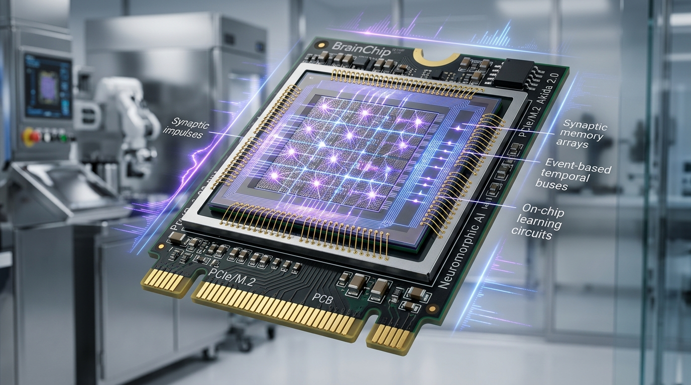
The physical architecture of the Akida 2.0 processor is structured as a scalable, two-dimensional mesh of autonomous Neuromorphic Processing Nodes (NPNs). Each NPN contains a cluster of specialized event-based execution engines tightly coupled with localized, distributed static RAM (SRAM) arrays for storing synaptic weights and neuron membrane potentials:
+-----------------------------------------------------------------------+
|                    BrainChip Akida 2.0 Core Mesh Fabric               |
+-----------------------------------------------------------------------+
|  +--------------------+  +--------------------+  +-----------------+  |
|  | Host Interface     |  | Event Generator    |  | Direct Sensor   |  |
|  | PCIe Gen 3 / I2C   |  | & Pixel-to-Spike   |  | Interface       |  |
|  | Control Block      |  | Converter (DVS/PCM)|  | (DVP, I2S, SPI) |  |
|  +---------+----------+  +---------+----------+  +--------+--------+  |
|            |                       |                      |           |
|  +---------v-----------------------v----------------------v--------+  |
|  |       Asynchronous Packetized Event Network-on-Chip (NoC)       |  |
|  +-----------------------------------------------------------------+  |
|        |                  |                  |                  |     |
|  +-----v-----+      +-----v-----+      +-----v-----+      +-----v-----+  |
|  | Node [0,0]|<---->| Node [0,1]|<---->| Node [0,2]|<---->| Node [0,3]|  |
|  | - 1024 Neu|      | - 1024 Neu|      | - 1024 Neu|      | - 1024 Neu|  |
|  | - Syn SRAM|      | - Syn SRAM|      | - Syn SRAM|      | - Syn SRAM|  |
|  | - TENN Eng|      | - TENN Eng|      | - TENN Eng|      | - TENN Eng|  |
|  +-----+-----+      +-----+-----+      +-----+-----+      +-----+-----+  |
|        ^                  ^                  ^                  ^     |
|        |                  |                  |                  |     |
|  +-----v-----+      +-----v-----+      +-----v-----+      +-----v-----+  |
|  | Node [1,0]|<---->| Node [1,1]|<---->| Node [1,2]|<---->| Node [1,3]|  |
|  | - 1024 Neu|      | - 1024 Neu|      | - 1024 Neu|      | - 1024 Neu|  |
|  | - Syn SRAM|      | - Syn SRAM|      | - Syn SRAM|      | - Syn SRAM|  |
|  | - TENN Eng|      | - TENN Eng|      | - TENN Eng|      | - TENN Eng|  |
|  +-----------+      +-----------+      +-----------+      +-----------+  |
+-----------------------------------------------------------------------+ Rather than broadcasting global multi-bit activations, NPNs communicate exclusively through an asynchronous, packetized Event Network-on-Chip (NoC). When a neuron reaches its excitation threshold, it generates an event packet containing only the originating neuron’s coordinate address and a discrete event magnitude (1, 2, or 4 bits). This Address Event Representation (AER) protocol transmits sparse, low-bandwidth routing packets across adjacent mesh routers only when physical spikes occur.
The Leaky Integrate-and-Fire (LIF) Neuron and Spiking Arithmetic
In conventional GPUs and NPUs, executing a neuron requires fetching floating-point weights and inputs, calculating their scalar product, and passing the result through a complex transcendental activation function (such as SiLU, GELU, or Softmax). In the Akida 2.0 microarchitecture, continuous activations are transformed into discrete temporal spikes governed by a digital Leaky Integrate-and-Fire (LIF) formulation.
Let $V_i[t]$ denote the discrete internal membrane potential of neuron $i$ at time step $t$. The temporal update equation implemented directly by Akida’s hardware state machine is expressed as:
$$V_i[t] = \beta \cdot V_i[t - 1] + \sum_{j \in \mathcal{P}i} W{ij} \cdot S_j[t] - \theta \cdot S_i[t - 1]$$
where:
- $\beta \in [0, 1)$ represents the programmable membrane leak decay constant, implemented in hardware via bitwise arithmetic shifts ($\beta = 1 - 2^{-k}$).
- $\mathcal{P}_i$ represents the set of presynaptic neurons connected to neuron $i$.
- $W_{ij} \in {-128, \dots, +127}$ represents the integer synaptic weight connecting presynaptic neuron $j$ to postsynaptic neuron $i$.
- $S_j[t] \in {0, 1}$ represents the incoming binary event spike from presynaptic neuron $j$.
- $\theta$ represents the firing threshold voltage.
- $S_i[t]$ is the output spike indicator function:
$$S_i[t] = \begin{cases} 1 & \text{if } V_i[t] \ge \theta \ 0 & \text{if } V_i[t] < \theta \end{cases}$$
Notice the fundamental mathematical property of this equation: when $S_j[t] = 0$ (no spike event), the product $W_{ij} \cdot S_j[t]$ evaluates to zero without performing any arithmetic calculation. When $S_j[t] = 1$, the hardware merely executes an integer addition:
$$V_i[t] \leftarrow V_i[t] + W_{ij}$$
By replacing multi-bit floating-point multiplications ($\text{FP32} \times \text{FP32}$) with simple localized integer additions, Akida reduces arithmetic energy consumption per synaptic operation by more than 99% compared to traditional GPU Tensor Cores.
Temporal Event-Based Neural Networks (TENN) Engine
While Spiking Neural Networks excel at static classification and spatial feature extraction, processing complex time-series signals—such as audio speech recognition, radar tracking, and multi-sensor predictive maintenance—traditionally demanded bulky transformer architectures.
To solve this dilemma without incurring transformer memory overhead, Akida 2.0 introduces the Temporal Event-Based Neural Network (TENN) engine. A TENN is a bio-inspired sequential model that processes streaming one-dimensional temporal signals using compact, multi-scale temporal convolutions over event streams.
Mathematically, a TENN layer applies a causal, dilated temporal filter bank $K \in \mathbb{R}^{C_{out} \times C_{in} \times L}$ to incoming event streams $X[t]$:
$$Y_c[t] = \sum_{k=0}^{L-1} \sum_{j=1}^{C_{in}} K_{c,j}[k] \cdot X_j[t - k \cdot d]$$
where $L$ is the temporal filter length and $d$ is the dilation rate.
Unlike standard transformers that compute global self-attention across an entire context window ($QK^T / \sqrt{d_k}$), the TENN engine evaluates temporal dependencies using sliding event-state buffers maintained directly within local on-chip SRAM:
| Attribute | Transformer Self-Attention | Recurrent Neural Net (LSTM) | Akida 2.0 TENN Engine |
|---|---|---|---|
| Computational Complexity | $\mathcal{O}(N^2)$ (Quadratic in sequence length) | $\mathcal{O}(N)$ (Sequential matrix-vector) | $\mathcal{O}(N)$ (Linear, Event-Sparse) |
| Memory Buffer Footprint | Gigabytes of KV Cache | Kilobytes of Hidden States | < 100 Kilobytes On-Chip SRAM |
| Arithmetic Primitive | Dense FP16 Matrix GEMM | Dense FP32/INT8 GEMV | Sparse Integer Add-Accumulate |
| Latency Scaling | High Time-to-First-Token | High Sequential Step Delay | Sub-Millisecond Streaming |
| Typical Power Dissipation | 50W - 400W | 5W - 25W | Sub-100 Milliwatts (< 0.1W) |
By eliminating the massive key-value cache and quadratic attention matrices, the TENN engine enables Akida 2.0 to run real-time keyword spotting, acoustic vibration analysis, and anomaly detection on edge microcontrollers with orders-of-magnitude lower memory and power consumption.
On-Chip Learning and Synaptic Plasticity Circuits
A distinguishing microarchitectural feature of the Akida 2.0 processor is its ability to perform autonomous on-chip learning. In conventional deep learning accelerators, learning requires backpropagation: computing loss gradients, calculating backward Jacobian matrices across all layers, and updating billions of parameters using gradient descent optimizers (such as AdamW or SGD). Backpropagation is computationally prohibitive for edge devices due to its intense memory footprint and floating-point requirements.
Akida 2.0 bypasses backpropagation by implementing biologically inspired Spike-Timing-Dependent Plasticity (STDP) and competitive Hebbian learning directly in hardware. In the final fully connected output layers, synaptic weights are updated based on the relative timing of presynaptic and postsynaptic spikes:
$$\Delta W_{ij} = \begin{cases} A_+ \exp\left(-\frac{\Delta t}{\tau_+}\right) & \text{if } \Delta t > 0 \quad (\text{Causal: presynaptic spike precedes postsynaptic}) \ -A_- \exp\left(\frac{\Delta t}{\tau_-}\right) & \text{if } \Delta t < 0 \quad (\text{Acausal: postsynaptic spike precedes presynaptic}) \end{cases}$$
where $\Delta t = t_{post} - t_{pre}$ represents the inter-spike arrival interval, $A_+$ and $A_-$ are learning rate amplitudes, and $\tau_+$ and $\tau_-$ are synaptic decay constants.
In hardware, Akida approximates this exponential curve using discrete, integer lookup tables and localized shift registers. When an edge device encounters a new visual defect on an industrial conveyor line or a new personalized speaker voice, the host application triggers an on-chip training pulse. The Akida chip binds the incoming sensory event pattern to an unassigned output neuron by updating its local synaptic SRAM weights in a single forward pass—enabling instant one-shot and few-shot learning with zero cloud connectivity.
Practical Implementation: Compiling SNNs and On-Chip Edge Learning with MetaTF
Transitioning from standard PyTorch or TensorFlow neural network models to optimized neuromorphic execution on Akida 2.0 is managed through BrainChip’s MetaTF software ecosystem. MetaTF includes model quantization tools, CNN-to-SNN conversion compilers, and the Akida Runtime (Akida-RT) Python and C++ APIs.
Model Conversion, Quantization, and Compilation Pipeline
The following Python script demonstrates how to load a standard pre-trained vision model (such as MobileNetV2 or an industrial classifier), convert its continuous activation layers into discrete Akida-compatible spiking layers using the Akida Model Zoo tools, and compile the final executable binary for the Akida 2.0 neuromorphic core:
#!/usr/bin/env python3
# BrainChip Akida 2.0 Neuromorphic Model Compilation and SNN Conversion Pipeline
# Converts a pre-trained CNN into a quantized Spiking Neural Network (SNN) executable.

import os
import sys
import numpy as np
import tensorflow as tf
import akida
import cnn2snn

def build_and_compile_akida_model(
    keras_model_path: str,
    output_akida_path: str,
    weight_bits: int = 4,
    activation_bits: int = 4
):
    print(f"[MetaTF] Loading pre-trained floating-point model from: {keras_model_path}")
    base_model = tf.keras.models.load_model(keras_model_path)

    # 1. Quantize Keras Model to Low-Bit Precision (Akida native supports 1, 2, 4 bits)
    print(f"[MetaTF] Quantizing model weights to {weight_bits}-bit and activations to {activation_bits}-bit...")
    quantized_model = cnn2snn.quantize(
        base_model,
        weight_bits=weight_bits,
        activation_bits=activation_bits
    )

    # 2. Convert Quantized CNN to Spiking Neural Network (SNN) Representation
    print("[MetaTF] Converting convolutional layers to event-driven Leaky Integrate-and-Fire nodes...")
    snn_model = cnn2snn.convert(quantized_model)
    print("[MetaTF] SNN graph conversion complete. Summary:")
    snn_model.summary()

    # 3. Target Akida 2.0 Hardware Device and Compile
    print("[MetaTF] Mapping spiking neurons to Akida 2.0 Neuromorphic Processing Node (NPN) mesh...")
    akida_device = akida.Device() # Detects connected PCIe / M.2 hardware or launches cycle-accurate simulator
    print(f"[MetaTF] Detected Hardware: {akida_device.desc}")

    # Compile the SNN model for the physical Akida hardware architecture
    compiled_akida_model = akida_device.map(snn_model)

    # 4. Save Compiled Hardware Binary
    compiled_akida_model.save(output_akida_path)
    print(f"[MetaTF] Hardware binary successfully exported to: {output_akida_path}")

    return compiled_akida_model

if __name__ == "__main__":
    # Example execution converting an industrial edge classifier
    build_and_compile_akida_model(
        keras_model_path="defect_classifier_mobilenet.h5",
        output_akida_path="defect_classifier_akida2.fbz",
        weight_bits=4,
        activation_bits=4
) On-Chip Few-Shot Edge Learning Implementation
One of Akida’s most powerful capabilities is continuous learning in the field. The following Python application demonstrates how an edge device deployed in a remote factory can learn a brand-new object class (such as a previously unseen defective component) directly on the physical Akida 2.0 silicon without retraining in the cloud:
#!/usr/bin/env python3
# BrainChip Akida 2.0 On-Chip Edge Learning Demonstration
# Implements one-shot / few-shot learning of new classes using hardware synaptic plasticity.

import numpy as np
import akida
import time

class AkidaEdgeLearner:
    def __init__(self, model_binary_path: str):
        print(f"[Akida-RT] Loading compiled neuromorphic binary: {model_binary_path}")
        self.model = akida.Model(model_binary_path)

        # Verify that the final layer is configured for on-chip hardware learning
        self.learning_layer = self.model.layers[-1]
        if not hasattr(self.learning_layer, 'learn'):
            raise RuntimeError("Final layer must be an Akida hardware learning layer (e.g., FullyConnected with plasticity)")

        print("[Akida-RT] Hardware learning layer verified. Ready for real-time edge adaptation.")

    def run_inference(self, input_features: np.ndarray) -> int:
        """Executes ultra-low-power event-driven forward pass."""
        # Convert input to unsigned 8-bit integer tensor format
        inputs_uint8 = np.clip(input_features, 0, 255).astype(np.uint8)

        start_time = time.perf_counter_ns()
        predictions = self.model.predict(inputs_uint8)
        latency_us = (time.perf_counter_ns() - start_time) / 1000.0

        predicted_class = np.argmax(predictions)
        confidence = predictions[0][predicted_class]

        print(f"[Inference] Class: {predicted_class} | Confidence: {confidence:.2f} | Latency: {latency_us:.1f} us")
        return predicted_class

    def learn_new_class_on_chip(self, training_samples: np.ndarray, target_class_id: int):
        """
        Updates synaptic weights in physical on-chip SRAM via hardware STDP plasticity.
        No backpropagation or cloud compute required.
        """
        print(f"[On-Chip Learning] Teaching Akida 2.0 new Class ID {target_class_id} using {len(training_samples)} sample(s)...")
        samples_uint8 = np.clip(training_samples, 0, 255).astype(np.uint8)

        start_time = time.perf_counter()

        # Trigger physical synaptic weight adaptation in hardware
        for sample in samples_uint8:
            sample_batch = np.expand_dims(sample, axis=0)
            self.learning_layer.fit(sample_batch, target_class_id)

        learn_duration_ms = (time.perf_counter() - start_time) * 1000.0
        print(f"[On-Chip Learning] Synaptic weights updated in physical hardware in {learn_duration_ms:.2f} ms.")

if __name__ == "__main__":
    # Initialize edge learner
    learner = AkidaEdgeLearner("defect_classifier_akida2.fbz")

    # Generate synthetic input simulating a new defect pattern
    synthetic_sample = np.random.randint(0, 256, size=(1, 224, 224, 3), dtype=np.uint8)

    # 1. Run baseline inference (unseen object class)
    print("\n--- Running Baseline Pre-Learning Inference ---")
    learner.run_inference(synthetic_sample)

    # 2. Perform instantaneous on-chip learning of new class (Class 9)
    print("\n--- Triggering On-Chip Hardware Learning ---")
    training_batch = np.repeat(synthetic_sample, 3, axis=0) # 3-shot learning
    learner.learn_new_class_on_chip(training_batch, target_class_id=9)

    # 3. Verify that Akida now immediately recognizes the new class
    print("\n--- Running Post-Learning Verification Inference ---")
    verified_class = learner.run_inference(synthetic_sample)
    assert verified_class == 9, "Hardware learning verification failed!"
print("[Success] Akida 2.0 successfully adapted its on-chip neural weights to recognize the new class!") Organizations building autonomous data harvesting agents or real-time web intelligence fleets can integrate neuromorphic edge devices with automated web scraping pipelines to harvest updated training corpora, cross-reference visual detections, and synchronize localized telemetry with central repositories. For a broader perspective on how neuromorphic hardware interfaces with enterprise data backbones, explore our AI engineering knowledge hub.
Architectural Comparison: BrainChip Akida 2.0 vs. Competing Edge AI Hardware
To understand where BrainChip Akida 2.0 fits within the rapidly expanding edge AI silicon landscape, hardware architects must evaluate its performance against prominent alternatives: conventional embedded GPUs (such as the NVIDIA Jetson Nano), specialized edge TPUs (such as Google Coral), conventional low-power edge NPUs (such as Hailo-8), and research neuromorphic chips (such as Intel Loihi 2).
| Architectural Feature | BrainChip Akida 2.0 | NVIDIA Jetson Nano | Google Coral Edge TPU | Hailo-8 M.2 NPU | Intel Loihi 2 (Research) |
|---|---|---|---|---|---|
| Computing Paradigm | Event-Driven Neuromorphic (SNN/TENN) | Synchronous SIMT GPU (Clocked) | Synchronous Systolic Array | Spatial Structure-Defined Dataflow | Asynchronous Spiking Neuromorphic |
| Semiconductor Node | Standard Digital CMOS (16nm/28nm) | TSMC 12nm FinFET | TSMC 28nm Planar | TSMC 16nm FinFET | Intel 4 (EUV Process) |
| Typical Power Envelope | 1 mW - 100 mW (Sub-milliwatt idle) | 5.0W - 10.0W | 2.0W - 2.5W | 2.5W - 5.0W | ~10 mW - 50 mW |
| Arithmetic Operators | Sparse Integer Additions (No Multipliers) | Dense FP16 / FP32 Tensor MACs | Dense INT8 Matrix MACs | Dense INT8 / INT16 MACs | Programmable Spiking Micro-code |
| Static / Idle Power | Near Zero (Events Drive Gates) | High Static Leakage | Moderate Static Power | Low Static Power | Near Zero |
| On-Chip Learning Support | Native Hardware Plasticity (STDP) | Backprop in Software (CPU/GPU) | None (Inference Only) | None (Inference Only) | Programmable Learning Rules |
| Temporal Processing (1D) | TENN Engine (Linear $\mathcal{O}(N)$ memory) | Transformers / RNNs (High DRAM) | TFLite 1D Convolutions | Fixed Dataflow Graph | Custom SNN Micro-kernels |
| Commercial Availability | Commercial Silicon & IP Licensing | Commercial Off-the-Shelf | Commercial Off-the-Shelf | Commercial Off-the-Shelf | Research Consortium Only |
| Cooling Requirement | Fanless / Zero Heatsink Needed | Active Fan / Bulky Aluminum Heatsink | Small Heatsink | Small Metal Heat-spreader | Passive Heat-sink |
Analysis of Architectural Trade-offs
A comprehensive examination of this scorecard illuminates the fundamental architectural trade-offs:
- Active vs. Event-Driven Power Consumption: While processors like the Hailo-8 and Google Coral deliver high raw TOPS metrics (26 TOPS and 4 TOPS, respectively), their synchronous architectures require continuous clock distribution and dense matrix processing. When an optical camera monitors an unchanging hallway or an industrial vibration sensor monitors a smoothly running motor, the Google Coral still draws roughly 2 watts. In contrast, Akida 2.0 draws less than 1 milliwatt in the absence of events—yielding an effective 2,000x efficiency advantage during quiescent monitoring periods.
- Standard CMOS Manufacturing vs. Exotic Neuromorphic Silicon: Unlike research neuromorphic chips that rely on specialized proprietary fabrication technologies (such as Intel Loihi 2 or analog memristor research chips), Akida 2.0 is synthesized entirely from standard digital CMOS cell libraries. This enables BrainChip to license Akida as a synthesizable IP core for integration into custom customer SoCs (System-on-Chips) across any major foundry (TSMC, GlobalFoundries, Samsung).
- Autonomous Edge Plasticity: Standard edge accelerators (Coral, Jetson, Hailo) are strictly static inference engines. If operational conditions shift in the field, these systems must collect data, serialize it over the network, retrain in the cloud, re-quantize the weights, and push a multi-megabyte firmware update. Akida 2.0 allows field technicians to train new classes directly on the device with a handful of samples in milliseconds, providing unmatched operational adaptability.
Production Engineering: Hardware Integration, Reliability, and Operational Telemetry
Transitioning BrainChip Akida 2.0 from laboratory prototyping into commercial production deployments requires rigorous attention to electrical power decoupling, sensor interface clocking, and automated hardware telemetry monitoring.
Physical Interfaces, Form Factors, and Electrical Guidelines
Akida 2.0 silicon is distributed in multiple physical formats: as standalone semiconductor dies, PCIe/M.2 accelerator cards, and synthesizable Verilog/VHDL IP cores. When integrating Akida modules into industrial edge controllers or smart camera PCBs, hardware engineers should observe the following guidelines:
- Power Rail Decoupling and Slew-Rate Management: Because neuromorphic processors transition from near-zero idle states to full event-processing bursts in nanoseconds, transient current demands ($dI/dt$) can induce voltage ripple on internal supply rails ($V_{dd} \approx 0.8\text{V}$ to $1.0\text{V}$). Place low-ESR ceramic decoupling capacitors ($0.1,\mu\text{F}$ and $10,\mu\text{F}$) directly adjacent to the power package balls to suppress high-frequency switching noise.
- Direct Sensor Integration (DVS and I2S): For maximum system energy efficiency, connect Akida directly to native event-based sensors—such as Dynamic Vision Sensors (DVS event cameras) or pulse-density modulated (PDM) MEMS microphones. Bypassing traditional frame-grabber controllers and feeding asynchronous spike streams directly into Akida’s event ingestion ports eliminates frame serialization latency and saves hundreds of milliwatts of system power.
- Thermal Management in Enclosed Enclosures: Because Akida 2.0 dissipates less than 100 milliwatts under full operational load, it does not require chassis fans, heat pipes, or external metal heatsinks. The module can be encapsulated within hermetically sealed, IP69K-rated industrial washdown enclosures or implanted medical housings without risk of thermal trapping.
Production Telemetry and Neuromorphic Health Daemon
In mission-critical enterprise fleets, an automated background service must monitor neuromorphic hardware health, tracking event firing rates, on-chip SRAM parity integrity, junction temperature, and synaptic plasticity allocations. The following Python daemon demonstrates an automated operational monitor that interfaces with the Akida hardware management API:
#!/usr/bin/env python3
# BrainChip Akida 2.0 Fleet Health and Event Telemetry Daemon
# Monitors event firing rates, SRAM parity, and silicon operational status.

import time
import logging
import json
import sys
from typing import Dict, Any

# Mock or production import of Akida Management API
try:
    import akida_mgmt as akm
except ImportError:
    # Simulated management interface for standalone testing
    class MockAkidaMgmt:
        class Device:
            def __init__(self, idx): self.idx = idx
            def get_temperature_celsius(self): return 34.2
            def get_power_consumption_mw(self): return 14.8
            def get_events_per_second(self): return 428000
            def get_sram_parity_errors(self): return 0
            def get_active_spiking_neurons(self): return 8192
            def get_plasticity_updates_count(self): return 12
            def reset_event_counters(self): pass
            def throttle_input_events(self): pass

        @staticmethod
        def init(): pass
        @staticmethod
        def device_count(): return 1
        @staticmethod
        def get_device(idx): return MockAkidaMgmt.Device(idx)
    akm = MockAkidaMgmt

logging.basicConfig(
    level=logging.INFO,
    format='%(asctime)s [%(levelname)s] [AKIDA-MONITOR] %(message)s',
    handlers=[logging.StreamHandler(sys.stdout)]
)

class AkidaHealthMonitor:
    def __init__(self, poll_interval_sec: float = 2.0, max_event_rate: int = 50_000_000):
        self.interval = poll_interval_sec
        self.max_event_rate = max_event_rate
        akm.init()
        self.num_devices = akm.device_count()
        self.devices = [akm.get_device(i) for i in range(self.num_devices)]
        logging.info(f"Initialized Akida Monitor for {self.num_devices} detected Neuromorphic Processing Unit(s).")

    def collect_telemetry(self, dev) -> Dict[str, Any]:
        """Polls real-time hardware telemetry from the Akida neuromorphic die."""
        temp = dev.get_temperature_celsius()
        power_mw = dev.get_power_consumption_mw()
        event_rate = dev.get_events_per_second()
        parity_errs = dev.get_sram_parity_errors()
        active_neurons = dev.get_active_spiking_neurons()
        plastic_updates = dev.get_plasticity_updates_count()

        return {
            "device_id": dev.idx,
            "junction_temp_c": temp,
            "power_mw": power_mw,
            "events_per_sec": event_rate,
            "sram_parity_errors": parity_errs,
            "active_neurons": active_neurons,
            "plasticity_updates": plastic_updates
        }

    def verify_operational_guards(self, dev, telemetry: Dict[str, Any]):
        """Evaluates hardware safety thresholds and detects event saturation."""
        event_rate = telemetry["events_per_sec"]
        dev_id = telemetry["device_id"]

        # Detect Event Storm (Sensory Noise Saturation)
        if event_rate >= self.max_event_rate:
            logging.warning(
                f"Device {dev_id} experiencing Event Storm ({event_rate} events/sec)! "
                "Throttling event input sensitivity to prevent NoC congestion."
            )
            dev.throttle_input_events()

        # Check SRAM Parity Integrity
        if telemetry["sram_parity_errors"] > 0:
            logging.error(f"Device {dev_id} detected {telemetry['sram_parity_errors']} synaptic SRAM parity faults!")

    def run_monitor(self):
        """Continuous execution loop exporting telemetry to Prometheus / FluentBit."""
        logging.info("Starting Akida neuromorphic monitoring loop...")
        try:
            while True:
                for dev in self.devices:
                    telemetry = self.collect_telemetry(dev)
                    self.verify_operational_guards(dev, telemetry)
                    logging.info(f"Telemetry Status: {json.dumps(telemetry)}")
                time.sleep(self.interval)
        except KeyboardInterrupt:
            logging.info("Terminating Akida Monitor cleanly.")

if __name__ == "__main__":
    monitor = AkidaHealthMonitor(poll_interval_sec=5.0)
    # Perform single initial diagnostic pass
    for dev in monitor.devices:
        stats = monitor.collect_telemetry(dev)
        print("\n=== Initial BrainChip Akida 2.0 Hardware Telemetry Pass ===")
        for k, v in stats.items():
            print(f"  {k:24s}: {v}")
        print("===========================================================\n")
print("Pre-flight diagnostic passed. Device ready for continuous autonomous edge service.") Production Readiness Verification Checklist
Prior to deploying BrainChip Akida 2.0 processors into commercial mass-production systems, hardware and systems engineering teams must verify each operational milestone:
- Sensor-to-Spike Noise Calibration: Calibrate dynamic vision sensor or acoustic microphone threshold levels in the target operating environment to ensure ambient background noise does not trigger unnecessary event spikes.
- Quantization Iso-Accuracy Validation: Run comprehensive accuracy validation across at least 2,000 real-world edge test samples, confirming that the 4-bit/2-bit quantized SNN achieves within 1.0% of the floating-point baseline model accuracy.
- On-Chip Learning Retention Testing: For systems utilizing edge synaptic plasticity, verify that continuous on-chip learning updates do not induce catastrophic forgetting across previously established base classification categories.
- Thermal and Power Cycling Longevity: Subject the hardware assembly to a 100-hour continuous stress cycle under maximum ambient temperatures (up to 85°C industrial rating), confirming zero memory bit flips or hardware resets.
BrainChip Akida 2.0 heralds a decisive shift in how edge artificial intelligence is conceived and deployed. By trading synchronous clocks and dense floating-point matrices for event-based spiking dynamics, temporal kernels, and native on-chip plasticity, Akida breaks through the von Neumann energy barrier. For developers and architects engineering the next generation of battery-operated, always-vigilant intelligent devices, neuromorphic event-based processing is no longer a distant theoretical vision—it is an accessible, silicon-proven reality.