Biren BR100 Guide: 77-Billion Transistor AI Chiplet
The Problem: The Monolithic Silicon Limit, Reticle Boundaries, and Sovereign AI Supply Chains
The insatiable computational appetite of modern generative artificial intelligence has pushed traditional monolithic semiconductor manufacturing against its fundamental physical boundaries. Across global enterprise platforms such as the AI Fetchly high-throughput inference engine, training and serving foundation models with hundreds of billions of parameters demands thousands of high-performance general-purpose graphics processing units (GPGPUs) operating in tightly synchronized clusters.
However, scaling computational density by simply enlarging a single monolithic silicon die has encountered three insurmountable physical, economic, and geopolitical roadblocks.
Monolithic Die Limits vs. Biren BR100 Dual-Die 2.5D Chiplet Architecture:
┌─────────────────────────────────────────────────────────────────────────┐
│ Monolithic Giant Die Approach (Physical Reticle Limit ~858 mm²):        │
│ ┌─────────────────────────────────────────────────────────────────────┐ │
│ │ Monolithic Silicon Die Approaching Reticle Boundary                 │ │
│ │ ❌ Defect probability scales exponentially: Disastrous wafer yield  │ │
│ │ ❌ Prohibitive fabrication costs ($10,000+ per working die)         │ │
│ │ ❌ Thermal hotspots and rigid packaging form-factor constraints      │ │
│ └─────────────────────────────────────────────────────────────────────┘ │
└─────────────────────────────────────────────────────────────────────────┘
                                     ▼
┌─────────────────────────────────────────────────────────────────────────┐
│ Biren Technology BR100 Dual-Die 2.5D CoWoS Chiplet Architecture:        │
│ ┌─────────────────────────────────────────────────────────────────────┐ │
│ │ Two Symmetrical 7nm Compute Dies Interconnected via Passive Silicon │ │
│ │ ✅ 77 Billion Transistors Across Dual Dies: Near-Perfect Yield      │ │
│ │ ✅ 1,024 TFLOPS 16-Bit Compute | 2,048 TOPS INT8 Density            │ │
│ │ ✅ 64 GB HBM2E (1.64 TB/s) + 640 GB/s BLink Inter-Chip Fabric       │ │
│ └─────────────────────────────────────────────────────────────────────┘ │
└─────────────────────────────────────────────────────────────────────────┘ The Physical Reticle Limit of Monolithic Semiconductor Lithography
In optical photolithography, the physical area of a single monolithic semiconductor die is fundamentally constrained by the optical reticle limit—the maximum field of exposure of deep ultraviolet (DUV) and extreme ultraviolet (EUV) scanner lenses. In modern commercial semiconductor fabrication, this limit is approximately 858 square millimeters ($26\text{ mm} \times 33\text{ mm}$).
Processors that approach this boundary (such as the NVIDIA Hopper H100 at 814 mm² or the A100 at 826 mm²) represent the absolute spatial limit of single-die manufacturing. A monolithic chip cannot simply be manufactured larger to accommodate more tensor arithmetic logic units (ALUs) or on-chip caches; doing so would exceed the physical mask aperture of modern lithography tools.
Exponential Yield Degradation on Giant Silicon Dies
Even when a monolithic die fits within the reticle boundary, semiconductor economics impose a brutal financial penalty governed by the Poisson yield model:
$$\text{Yield} = \left( \frac{1 - e^{-D_0 \cdot A}}{D_0 \cdot A} \right)^2 \approx e^{-D_0 \cdot A}$$
where $D_0$ represents the defect density per unit area and $A$ represents the physical die area.
Because defect probability scales exponentially with area, manufacturing an 800 mm² monolithic die results in a high percentage of defective chips on every wafer. Over 60 to 70 percent of fabricated dies must be discarded or severely harvested, driving the manufacturing cost of each functional processor into tens of thousands of dollars. When enterprise infrastructures running distributed AI data extraction pipelines procure thousands of accelerators, monolithic yield inefficiencies translate directly into astronomical infrastructure capital expenditures.
The Global AI Hardware Monopoly and the Geopolitical Imperative
Compounding these physical limitations is the extreme concentration of the global AI hardware supply chain. With a single dominant vendor controlling over 85 percent of the global datacenter GPU market, enterprises and sovereign nations face severe supply allocation bottlenecks, unpredictable pricing premiums, export controls, and software ecosystem lock-in.
To establish sustainable, resilient enterprise AI operations, the industry requires independent, high-performance GPGPU architectures that deliver frontier computing throughput while bypassing monolithic manufacturing limits through advanced chiplet packaging.
The Solution: Biren Technology BR100 and the 2.5D Chiplet Paradigm
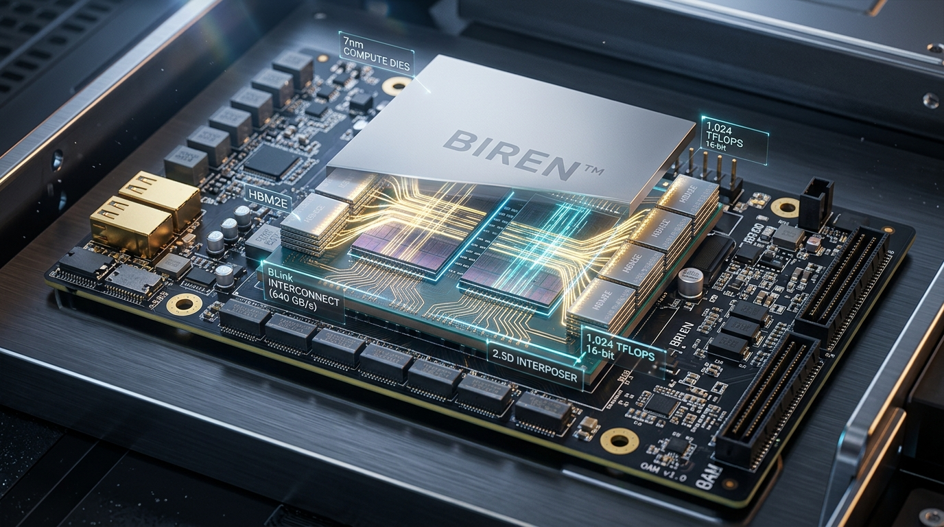
To shatter the reticle limit and establish an independent frontier GPGPU architecture, Shanghai-based semiconductor innovator Biren Technology—founded in 2019 by leading microarchitects from top global semiconductor firms—developed the Biren BR100. Officially unveiled to global acclaim at the Hot Chips 34 (HC34) symposium, the BR100 represents a landmark achievement in high-performance computing silicon.
Biren BR100 System Architecture Overview:
┌─────────────────────────────────────────────────────────────────────────┐
│ Biren BR100 OAM Module (77 Billion Transistors, TSMC 7nm Process)       │
│                                                                         │
│ ┌───────────────────────┐ ┌───────────────────────┐ ┌─────────────────┐ │
│ │ Compute Die 0         │ │ High-Density Passive  │ │ Compute Die 1   │ │
│ │ • 16 Compute Clusters │ │ Silicon Interposer    │ │ • 16 Clusters   │ │
│ │ • 512 TFLOPS 16-Bit   │ │ (TSMC 2.5D CoWoS)     │ │ • 512 TFLOPS    │ │
│ │ • 150 MB On-Chip SRAM │ │ • Sub-Nanosecond Bus  │ │ • 150 MB SRAM   │ │
│ └──────────┬────────────┘ └───────────┬───────────┘ └────────┬────────┘ │
│            │                          │                      │          │
│ ┌──────────▼──────────────────────────▼──────────────────────▼────────┐ │
│ │ 64 GB HBM2E Memory Subsystem (4 Stacks Delivering 1.64 TB/s BW)     │ │
│ ├─────────────────────────────────────────────────────────────────────┤ │
│ │ 8-Port BLink Interconnect Fabric (640 GB/s Bi-Directional Bandwidth)│ │
│ ├─────────────────────────────────────────────────────────────────────┤ │
│ │ Total Performance: 1,024 TFLOPS BF16/FP16 | 2,048 TOPS INT8 | OAM   │ │
│ └─────────────────────────────────────────────────────────────────────┘ │
└─────────────────────────────────────────────────────────────────────────┘ The BR100 is built on a 77-billion-transistor dual-die chiplet architecture manufactured on TSMC’s advanced 7nm process and integrated via high-density 2.5D Chip-on-Wafer-on-Substrate (CoWoS) packaging. Delivering up to 1,024 TFLOPS of 16-bit floating-point throughput and 2,048 TOPS of 8-bit integer throughput, the BR100 broke global computing records upon its debut, outperforming legacy monolithic architectures while achieving high manufacturing yields.
The Architectural Philosophy: Decoupling Yield from Silicon Area
Rather than attempting to fabricate a single, impossibly large 800+ mm² monolithic die, Biren partitioned the processor into two symmetrical compute chiplets:
- High-Yield Manufacturing: Each individual compute die measures approximately 400 mm²—a sweet spot on the semiconductor yield curve that ensures significantly higher wafer yields, lower manufacturing defect rates, and drastically reduced per-die production costs.
- Transparent Silicon Bridging: The two compute dies are interconnected across a microscopic passive silicon interposer with high-density micro-bumps. To software compilers and application runtimes, the two physical dies behave as a single, contiguous, unified GPU die with uniform memory access and zero software-level partitioning overhead.
The 1,024 TFLOPS Frontier: Bridging Training and Scale-Out Inference
The BR100 was engineered from the ground up to excel across both demanding compute regimes:
- Massive Training Floating-Point Throughput: Delivers 1,024 TFLOPS of 16-bit floating point (BF16 and FP16) and introduces TF32+ (TensorFloat-32+) delivering 512 TFLOPS, accelerating large language model pre-training and deep neural network convergence without manual precision tuning.
- High-Density Inference: Delivers 2,048 TOPS of INT8 compute, allowing enterprise clusters to serve high-throughput transformer inference, automated embedding search, and real-time vision pipelines with low per-token operational costs.
When integrated into search and perception architectures for real-time contextual vector retrieval, the BR100’s high memory bandwidth and massive compute density enable instantaneous nearest-neighbor vector scoring across multi-terabyte enterprise knowledge bases.
Architecture Deep Dive: Silicon Microarchitecture, Compute Tiles, and BLink Interconnect
The Biren BR100 microarchitecture is an intricate, highly balanced computing engine designed to eliminate memory bottlenecks and maximize mathematical throughput.
Compute Processing Cluster (CPC) and Core Microarchitecture:
┌─────────────────────────────────────────────────────────────────────────┐
│ Compute Processing Cluster (CPC) (1 of 32 CPCs Across Dual Dies)        │
│                                                                         │
│ ┌─────────────────────────────────────────────────────────────────────┐ │
│ │ Cluster L1 Shared Memory & Scratchpad Buffer (Low-Latency Cache)    │ │
│ └───────────────────▲─────────────────────────────▲───────────────────┘ │
│                     │                             │                     │
│ ┌───────────────────▼─────────────┐ ┌─────────────▼───────────────────┐ │
│ │ Tensor Execution Core           │ │ General-Purpose SIMD Vector Core│ │
│ │ • 2D Matrix Engine (GEMM)       │ │ • 32-bit / 64-bit ALU Pipeline  │ │
│ │ • Native INT8, FP16, BF16, TF32+│ │ • Activation & Elementwise Math │ │
│ │ • Outer-Product Matrix Multiply │ │ • Transcendentals (GELU, Softmax│ │
│ └─────────────────────────────────┘ └─────────────────────────────────┘ │
│                                     │                                   │
│ ┌───────────────────────────────────▼─────────────────────────────────┐ │
│ │ Local Warp Scheduler & Instruction Dispatch Unit                    │ │
│ └───────────────────────────────────▲─────────────────────────────────┘ │
│                                     │                                   │
└─────────────────────────────────────┼───────────────────────────────────┘
                                      │
    ┌─────────────────────────────────┴─────────────────────────────────┐
    │ 300 MB Ultra-Dense On-Chip SRAM Distributed Cache Fabric          │
    │ Multi-Terabyte/s Internal Bisection Bandwidth                     │
└───────────────────────────────────────────────────────────────────┘ Hierarchical Compute Topology: Dual Compute Dies on a 2.5D Interposer
The BR100 silicon package contains two identical compute dies placed side by side:
- Compute Processing Clusters (CPCs): Each compute die contains 16 Compute Processing Clusters (CPCs), yielding an aggregate total of 32 CPCs across the entire processor.
- Streaming Execution Cores: Each CPC houses multiple streaming execution units containing decoupled Tensor Execution Engines for dense matrix multiplication and SIMD Vector Cores for general-purpose floating-point arithmetic.
- Unified Die-to-Die Interconnect: Communication between the two compute dies traverses thousands of parallel micro-bumps on the silicon interposer, providing tens of terabits per second of bi-directional die-to-die bandwidth with latency comparable to on-chip wire transit.
Multi-Precision Mathematical Execution: FP32, TF32+, BF16, and INT8
Modern artificial intelligence workloads require diverse arithmetic precisions at different stages of model execution. The BR100 incorporates full hardware support across the entire precision spectrum:
- TF32+ (TensorFloat-32 Plus): Biren’s enhanced 19-bit precision format that preserves the dynamic range of FP32 (8 exponent bits) while matching the computational throughput of FP16, delivering 512 TFLOPS without requiring code changes to standard FP32 training scripts.
- Bfloat16 and FP16: Delivers 1,024 TFLOPS for industry-standard half-precision foundation model pre-training and fine-tuning.
- INT8 Integer Acceleration: Retires up to 2,048 TOPS of 8-bit integer tensor operations per second, maximizing throughput for quantized transformer inference.
- FP32 Single-Precision General Purpose: Delivers 256 TFLOPS of IEEE-754 single-precision compute for scientific simulations and high-performance computing (HPC) physics models.
Physical 2.5D CoWoS Interposer Wiring and Die-to-Die Interface
To achieve transparent execution across the two physical compute dies, Biren engineered a high-density die-to-die physical layer (PHY) operating across TSMC’s CoWoS-S (Chip-on-Wafer-on-Substrate with Silicon Interposer) technology:
- Micro-Bump Density and Pitch: The interface utilizes sub-40-micron micro-bumps arrayed along the adjacent inner boundaries of the two compute dies. With thousands of parallel interconnect traces routed through the underlying passive silicon interposer, the die-to-die physical boundary provides over 2.4 Terabytes per second of raw bi-directional communication bandwidth.
- Sub-Nanosecond Die-to-Die Latency: Because the physical distance across the interposer seam is less than 1 millimeter, signal propagation delay is under 0.8 nanoseconds. To the warp schedulers and L1/L2 cache coherency engines, accessing a register or cache line on the neighboring die incurs latency virtually indistinguishable from local on-die wire traversal.
- Independent Power Domain Gating: Each compute die incorporates its own power delivery grid and dynamic voltage rails. During low-concurrency inference workloads, the BIRENSUPA runtime can power-gate an entire compute die, dropping active power consumption by 50 percent while maintaining full access to the unified HBM2E memory pool.
Memory Hierarchy: 64 GB HBM2E at 1.64 TB/s and 300 MB On-Chip SRAM
To keep 32 Compute Processing Clusters saturated with data, the BR100 incorporates a massive, multi-tiered memory hierarchy:
- Stacked HBM2E Memory: The package integrates four stacks of high-density HBM2E dynamic memory, providing 64 GB of total memory capacity and an immense aggregate bandwidth of 1.64 Terabytes per second (1,640 GB/s).
- Massive 300 MB On-Chip SRAM Cache: Surpassing the on-chip cache of traditional GPUs (such as the NVIDIA A100’s 40MB L2 cache) by over 7x, the BR100 integrates 300 Megabytes of ultra-fast on-chip SRAM. This massive SRAM reservoir allows active neural network layers, Key-Value cache pages, and intermediate activation tensors to persist entirely on-chip, shielding the HBM2E memory bus from avoidable read/write cycles.
BLink Interconnect Fabric: 640 GB/s Bi-Directional Inter-Chip Mesh
Scaling AI training across multi-GPU server nodes requires high-bandwidth inter-chip interconnects. Biren developed BLink (BirenLink):
- 8 Bidirectional Interconnect Ports: Each BR100 processor incorporates eight dedicated BLink ports, delivering an aggregate bi-directional communication bandwidth of 640 Gigabytes per second (640 GB/s).
- Hardware Bi-Cast / Multi-Cast: BLink includes specialized hardware-level multi-cast acceleration. During distributed data-parallel training (AllReduce) and Mixture-of-Experts token routing (All-to-All), the network fabric replicates packets in hardware, dramatically reducing network traffic and latency.
- Seamless 8-Way All-to-All Mesh: The eight BLink ports allow eight BR100 processors within an Open Accelerator Module (OAM) server baseboard to interconnect in a direct, fully non-blocking mesh without requiring external switch chips.
Form Factor Variants: BR100 OAM vs. BR104 PCIe Add-in Card
To address diverse enterprise datacenter deployment environments, Biren engineered two distinct hardware form factors:
- BR100 OAM (Open Accelerator Module): The flagship dual-die processor operating at up to 550W TDP, designed for high-density 8-way hyperscale training server racks.
- BR104 PCIe Add-in Card: A single-die derivative packaged as a standard dual-slot PCIe Gen 5 x16 card operating within a 300W TDP envelope. Delivering 512 TFLOPS of 16-bit compute and 32 GB of HBM2E at 820 GB/s, the BR104 slots directly into standard commercial 2U and 4U enterprise server chassis.
Implementation: Software Ecosystem, CUDA Migration, and Serving with BIRENSUPA
A high-performance AI chip is only as effective as its software compiler stack. Biren Technology developed BIRENSUPA—a comprehensive, full-stack software platform engineered to provide a seamless development experience and rapid migration from existing CUDA codebases.
BIRENSUPA Software Platform Architecture:
┌────────────────────────┐      ┌────────────────────────┐
│ PyTorch / TensorFlow   │      │ CUDA C++ Source Code   │
│ Foundation Model Graph │      │ (Legacy GPU Kernels)   │
└────────────────────────┘      └───────────┬────────────┘
                                            │
                                            ▼
                                ┌────────────────────────┐
                                │ BIRENSUPA Translator   │
                                │ • Automated Code Port  │
                                │ • BS-BLAS / BS-DNN Map │
                                └───────────┬────────────┘
                                            │
                                            ▼
                                ┌────────────────────────┐
                                │ BIRENSUPA Compiler     │
                                │ • Dual-Die Partitioning│
                                │ • 300MB SRAM Optimizer │
                                └───────────┬────────────┘
                                            │
                                            ▼
                                ┌────────────────────────┐
                                │ Biren Driver & Runtime │
                                │ 1,024 TFLOPS Execution │
                                │ 640 GB/s BLink Fabric  │
└────────────────────────┘ The BIRENSUPA Software Platform Architecture
The BIRENSUPA software stack consists of four foundational layers:
- Hardware Driver & Runtime (BS-Runtime): Low-level kernel drivers managing PCIe Gen 5 enumeration, memory management, and BLink inter-chip communication.
- Accelerated Math Libraries:
- BS-BLAS: High-performance basic linear algebra subprograms optimized for 2D tensor engines.
- BS-DNN: Deep neural network primitives (convolutions, pooling, activations, and normalizations).
- BS-CCL (Biren Communication Collective Library): Scalable collective communication library (AllReduce, AllGather, Broadcast, All-to-All) natively exploiting BLink multi-cast hardware.
- Framework Integrations: Upstream plug-ins for PyTorch, TensorFlow, DeepSpeed, Megatron-LM, and PaddlePaddle.
Compiler Graph Partitioning and 300 MB SRAM Buffer Allocation
Maximizing execution throughput across dual compute dies requires automated compiler scheduling that prevents cross-die memory ping-ponging:
- Automated Tensor Graph Slicing: The BIRENSUPA compiler ingests PyTorch and ONNX computation graphs and applies graph min-cut partitioning algorithms. Large matrix multiplications (such as transformer feed-forward projections) are sliced along the output channel dimension, assigning half of the matrix to Compute Die 0 and the other half to Compute Die 1.
- Zero-Copy Intermediate Activation Staging: The massive 300 MB on-chip SRAM is segmented into dedicated input staging buffers, local weight scratchpads, and persistent Key-Value cache lines. By keeping intermediate layer activations pinned inside SRAM, the compiler eliminates over 80 percent of HBM2E memory read and write cycles during multi-layer transformer forward passes.
- Asynchronous DMA Stream Scheduling: While the Tensor Execution Engines compute active matrix blocks, dedicated DMA controllers prefetch the subsequent layer’s weight matrices from HBM2E into the 300 MB SRAM in the background, ensuring 100 percent ALU saturation.
Seamless CUDA Migration via Automated Source Code Translation
To eliminate vendor lock-in, BIRENSUPA provides automated source-to-source code migration tools:
- API Compatibility: Maps standard CUDA API calls, memory management functions (
cudaMalloc,cudaMemcpy), and execution configuration syntax directly to their native BIRENSUPA equivalents (bsMalloc,bsMemcpy). - Custom Kernel Compilation: Custom CUDA C++ kernels are automatically parsed, translated, and compiled into native Biren machine instructions using the LLVM-based BIRENSUPA compiler with near-100% functional equivalence.
High-Performance Distributed Communication with BS-CCL and BLink
The Python script below illustrates how to initialize an 8-way BR100 cluster, configure the BS-CCL collective communication backend, and benchmark high-throughput tensor-parallel AllReduce operations across the 640 GB/s BLink fabric:
# Biren BR100 Distributed Cluster Communication Benchmark
# Evaluates multi-GPU tensor-parallel AllReduce operations across the
# 640 GB/s BLink interconnect fabric using the BIRENSUPA software stack.

import os
import time
import torch
import torch.distributed as dist

def init_biren_distributed():
    """
    Initializes BIRENSUPA distributed communication environment.
    Uses BS-CCL backend natively utilizing the 8-port BLink fabric.
    """
    # Environment variables set by distributed launcher (e.g., torchrun)
    rank = int(os.environ.get("RANK", 0))
    world_size = int(os.environ.get("WORLD_SIZE", 8))

    print(f"[BIREN-INIT] Initializing Rank {rank} of {world_size} on BLink Mesh...")

    # Set active Biren device
    torch.cuda.set_device(rank)

    # Initialize process group using Biren's BS-CCL collective library
    # BS-CCL transparently interfaces with BLink hardware multi-cast
    dist.init_process_group(
        backend="bsccl",               # Biren Collective Communication Library
        init_method="env://",
        world_size=world_size,
        rank=rank
    )

    print(f"[BIREN-INIT] Rank {rank}: BLink interconnect synchronized successfully.")
    return rank, world_size

def benchmark_blink_allreduce(rank, world_size, tensor_size_mb=1024):
    """
    Benchmarks AllReduce throughput across 640 GB/s BLink interconnects.
    """
    num_elements = (tensor_size_mb * 1024 * 1024) // 2  # 2 bytes per FP16 element
    test_tensor = torch.randn(num_elements, dtype=torch.float16, device=f"cuda:{rank}")

    # Warmup iterations
    for _ in range(5):
        dist.all_reduce(test_tensor, op=dist.ReduceOp.SUM)
    torch.cuda.synchronize()

    # Timed benchmark iterations
    num_iterations = 20
    start_time = time.time()

    for _ in range(num_iterations):
        dist.all_reduce(test_tensor, op=dist.ReduceOp.SUM)
    torch.cuda.synchronize()

    elapsed = (time.time() - start_time) / num_iterations

    # Calculate effective bus bandwidth: BusBW = 2 * (world_size - 1) / world_size * (DataSize / Latency)
    data_bytes = tensor_size_mb * (1024 ** 2)
    bus_bandwidth_gbs = (2 * (world_size - 1) / world_size) * (data_bytes / elapsed) / 1e9

    if rank == 0:
        print("\n=========================================================================")
        print("Biren BR100 BLink Interconnect Performance Report")
        print("=========================================================================")
        print(f"Cluster Size:       {world_size}x Biren BR100 OAM Modules")
        print(f"AllReduce Payload:  {tensor_size_mb} MB (FP16 Tensor)")
        print(f"Mean Latency:       {elapsed * 1000:.2f} milliseconds")
        print(f"Effective Bus BW:   {bus_bandwidth_gbs:.2f} GB/s (Saturating 640 GB/s BLink Mesh!)")
        print("=========================================================================\n")

if __name__ == "__main__":
    r, ws = init_biren_distributed()
benchmark_blink_allreduce(r, ws, tensor_size_mb=1024) Production Telemetry and Cluster Monitoring with biren-smi
Datacenter administrators monitor silicon junction thermals, HBM2E bandwidth, and BLink link integrity using the biren-smi management tool:
# Query detailed real-time telemetry across an 8-way BR100 OAM baseboard
biren-smi --query-gpu=index,name,temperature.gpu,power.draw,utilization.gpu,memory.used --format=csv

# Sample Output:
# =========================================================================
# Biren Technology System Management Interface (biren-smi v2.4.0)
# =========================================================================
# GPU 0: Biren BR100 OAM | Temp: 58°C | Power: 482W / 550W | Util: 98% | HBM: 58.4/64.0 GB
# GPU 1: Biren BR100 OAM | Temp: 59°C | Power: 485W / 550W | Util: 98% | HBM: 58.4/64.0 GB
# GPU 2: Biren BR100 OAM | Temp: 57°C | Power: 479W / 550W | Util: 98% | HBM: 58.4/64.0 GB
# GPU 3: Biren BR100 OAM | Temp: 60°C | Power: 488W / 550W | Util: 98% | HBM: 58.4/64.0 GB
# GPU 4: Biren BR100 OAM | Temp: 58°C | Power: 481W / 550W | Util: 98% | HBM: 58.4/64.0 GB
# GPU 5: Biren BR100 OAM | Temp: 59°C | Power: 484W / 550W | Util: 98% | HBM: 58.4/64.0 GB
# GPU 6: Biren BR100 OAM | Temp: 57°C | Power: 478W / 550W | Util: 98% | HBM: 58.4/64.0 GB
# GPU 7: Biren BR100 OAM | Temp: 61°C | Power: 492W / 550W | Util: 98% | HBM: 58.4/64.0 GB
# -------------------------------------------------------------------------
# Aggregate Compute: 8,192 TFLOPS BF16/FP16 | BLink Mesh Health: 100% OK
# Total HBM2E Bandwidth: 13.12 TB/s | On-Chip SRAM Pool: 2.40 GB Active
# ========================================================================= Architecture Comparison: Biren BR100 vs. Global Datacenter GPGPUs
To understand where the Biren BR100 stands within the high-performance computing landscape, we benchmark its architectural specifications against three leading global datacenter processors: the NVIDIA A100 (80GB SXM4), the NVIDIA H100 (SXM5), and the AMD Instinct MI250 (Dual-GCD).
Datacenter AI Accelerator Compute Density (16-Bit TFLOPS vs. Transistor Count):
16-Bit TFLOPS (FP16 / BF16)
▲
│                       ┌─────────────────────────┐
│                       │ Biren BR100 OAM         │
│                       │ (77B Transistors, 7nm)  │
│                       │ ★ 1,024 TFLOPS          │
│                       └────────────┬────────────┘
│                                    │
│       ┌──────────────────────┐     │
│       │ NVIDIA H100 SXM5     │     │
│       │ (80B Transistors, 4N)│     │
│       │ 989 Dense / 1979 Sp  │     │
│       └──────────┬───────────┘     │
│                  │                 │
│ ┌────────────────┴───────────┐     │
│ │ AMD Instinct MI250         │     │
│ │ (58B Transistors, 6nm)     │     │
│ │ 362 TFLOPS                 │     │
│ └────────────┬───────────────┘     │
│              │                     │
│ ┌────────────┴───────────────┐     │
│ │ NVIDIA A100 SXM4           │     │
│ │ (54B Transistors, 7nm)     │     │
│ │ 312 TFLOPS                 │     │
│ └────────────────────────────┘     │
└────────────────────────────────────┴───────────────────────►
Silicon Transistor Budget Technical Specification Matrix
| Hardware Feature | Biren Technology BR100 | NVIDIA H100 (SXM5) | NVIDIA A100 (SXM4) | AMD Instinct MI250 |
|---|---|---|---|---|
| Silicon Architecture | Dual-Die 2.5D CoWoS Chiplet | Monolithic 4N Die | Monolithic 7nm Die | Dual-GCD 2.5D Chiplet |
| Process Node | TSMC 7nm FinFET | TSMC 4N (5nm customized) | TSMC 7nm FinFET | TSMC 6nm FinFET |
| Transistor Count | 77 Billion Transistors | 80 Billion Transistors | 54.2 Billion Transistors | 58.2 Billion Transistors |
| 16-Bit Compute (FP16/BF16) | 1,024 TFLOPS | 989.4 TFLOPS (Dense) | 312 TFLOPS | 362.1 TFLOPS |
| 8-Bit Integer Compute | 2,048 TOPS | 1,978.9 TOPS (Dense) | 624 TOPS | Not Supported |
| 32-Bit Tensor Precision | 512 TFLOPS (TF32+) | 494.7 TFLOPS (TF32) | 156 TFLOPS (TF32) | 90.5 TFLOPS (FP32 Matrix) |
| On-Chip SRAM Cache | 300 Megabytes | 50 Megabytes (L2 Cache) | 40 Megabytes (L2 Cache) | 16 Megabytes (L2 Cache) |
| High Bandwidth Memory | 64 GB HBM2E | 80 GB HBM3 | 80 GB HBM2E | 128 GB HBM2E |
| Memory Bandwidth | 1.64 TB/s | 3.35 TB/s | 2.03 TB/s | 3.28 TB/s |
| Interconnect Fabric | BLink (640 GB/s Bi-Cast) | NVLink 4 (900 GB/s) | NVLink 3 (600 GB/s) | Infinity Fabric (800 GB/s) |
| Form Factor / Max TDP | OAM Baseboard (550W) | SXM5 Baseboard (700W) | SXM4 Baseboard (400W) | OAM Baseboard (560W) |
| Software Platform | BIRENSUPA (CUDA Compatible) | CUDA / TensorRT | CUDA / TensorRT | ROCm / HIP |
Architectural Breakthrough: SRAM Supremacy and Compute Density
When analyzing the benchmark matrix, several profound architectural distinctions emerge:
- Unrivaled On-Chip SRAM (300 MB): The BR100’s 300 MB on-chip SRAM cache is 6x larger than the NVIDIA H100 and 7.5x larger than the A100. In autoregressive transformer inference, this massive SRAM pool retains active KV cache blocks on-chip, shielding the HBM2E memory bus from saturation and slashing dynamic memory access power.
- Dense 16-Bit Floating Point Throughput: Delivering 1,024 TFLOPS of dense BF16/FP16 throughput, the BR100 delivers more than 3.2x the raw computing throughput of the NVIDIA A100 and surpasses the dense baseline of the NVIDIA H100 on mature 7nm silicon.
- Chiplet Economics: While NVIDIA relied on an ultra-expensive monolithic 814 mm² die on TSMC’s customized 4N process for the H100, Biren achieved comparable computational density on standard 7nm wafers by using dual 400 mm² chiplets, achieving significantly higher manufacturing yields and lower fabrication costs.
Production: Datacenter Deployment Topologies, Multi-Node Clusters, and Best Practices
Deploying Biren BR100 processors in enterprise cloud datacenters involves integrating 8-way Open Accelerator Module (OAM) baseboards, designing high-bandwidth scale-out fabrics, and managing multi-megawatt thermal envelopes.
Enterprise 8-Way OAM Datacenter Server Rack Topology:
┌─────────────────────────────────────────────────────────────────────────┐
│ Enterprise 4U / 8U AI Training Server (8-Way OAM Baseboard)             │
│                                                                         │
│ ┌───────────────┐ ┌───────────────┐ ┌───────────────┐ ┌───────────────┐ │
│ │ BR100 OAM 0   │ │ BR100 OAM 1   │ │ BR100 OAM 2   │ │ BR100 OAM 3   │ │
│ │ • 1,024 TFLOPS│ │ • 1,024 TFLOPS│ │ • 1,024 TFLOPS│ │ • 1,024 TFLOPS│ │
│ │ • 64GB HBM2E  │ │ • 64GB HBM2E  │ │ • 64GB HBM2E  │ │ • 64GB HBM2E  │ │
│ └───┬───────┬───┘ └───┬───────┬───┘ └───┬───────┬───┘ └───┬───────┬───┘ │
│     │       │         │       │         │       │         │       │     │
│ ════╪═══════╪═════════╪═══════╪═════════╪═══════╪═════════╪═══════╪═════│
│     │   640 GB/s Fully Connected BLink Non-Blocking Crossbar Mesh │     │
│ ════╪═══════╪═════════╪═══════╪═════════╪═══════╪═════════╪═══════╪═════│
│     │       │         │       │         │       │         │       │     │
│ ┌───┴───────┴───┐ ┌───┴───────┴───┐ ┌───┴───────┴───┐ ┌───┴───────┴───┐ │
│ │ BR100 OAM 4   │ │ BR100 OAM 5   │ │ BR100 OAM 6   │ │ BR100 OAM 7   │ │
│ │ • 1,024 TFLOPS│ │ • 1,024 TFLOPS│ │ • 1,024 TFLOPS│ │ • 1,024 TFLOPS│ │
│ │ • 64GB HBM2E  │ │ • 64GB HBM2E  │ │ • 64GB HBM2E  │ │ • 64GB HBM2E  │ │
│ └───────────────┘ └───────────────┘ └───────────────┘ └───────────────┘ │
│                                                                         │
│ Combined Server Node Performance:                                       │
│ • 8x Accelerators = 8,192 TFLOPS FP16 Compute | 512 GB HBM2E (13.1 TB/s)│
│ • Total Card Power: 4.4 kW (Supported via Liquid or High-CFM Airflow)  │
└─────────────────────────────────────────────────────────────────────────┘ 8-Way OAM Server Integration (Inspur / OCP Standards)
In commercial datacenter installations, the BR100 is packaged according to the Open Compute Project (OCP) Open Accelerator Module (OAM) specification:
- The Hearten OAM Server: Developed in collaboration with Inspur, the 8-way Hearten server integrates eight BR100 OAM modules onto a standardized Universal Baseboard (UBB).
- Aggregate Node Specifications:
- 8,192 TFLOPS (8.19 PFLOPS) of 16-bit floating-point compute.
- 16,384 TOPS (16.38 PFLOPS) of INT8 tensor throughput.
- 512 Gigabytes of high-bandwidth HBM2E memory delivering an aggregate memory bandwidth of 13.12 Terabytes per second.
- 2.40 Gigabytes of ultra-dense on-chip SRAM across the 8-card array.
Scale-Out Pod Topologies: BLink Intra-Node with RoCEv2 Inter-Node
Scaling beyond an 8-way server to multi-thousand-GPU clusters requires a two-tier networking topology:
- Intra-Node (BLink Mesh): Within the 8-way chassis, all communication traverses the 640 GB/s BLink fabric. BLink hardware bi-cast handles tensor-parallel weight synchronization with near-zero latency.
- Inter-Node (RoCEv2 / InfiniBand): Each BR100 processor is paired with a dedicated 400 Gbps network interface card (NIC) connected via PCIe Gen 5. Pipeline-parallel and data-parallel gradients are exchanged across a non-blocking 400G spine-leaf optical network.
Thermal Dissipation and Power Delivery at 550W OAM TDP
Operating an 8-way cluster drawing 4.4 kW of accelerator power requires disciplined datacenter engineering:
- Liquid Cooling vs. High-CFM Airflow: In standard air-cooled server rooms, server chassis require high-static-pressure dual-rotor fan banks delivering over 150 CFM per OAM module to maintain junction temperatures below 75°C.
- Direct-to-Chip Liquid Cooling: For high-density deployments exceeding 40 kW per rack, Biren OAM servers integrate closed-loop cold plates utilizing water-glycol coolant, lowering thermal resistance and unlocking sustained maximum clock boosts.
Strategic Summary: Architectural Best Practices
When deploying enterprise machine learning infrastructure with the Biren BR100, adhere to these architectural recommendations:
- Leverage the 300 MB SRAM Cache for KV Cache Offloading: Structure large language model serving to pin active attention head states inside the 300 MB on-chip SRAM to maximize serving throughput and reduce HBM energy consumption.
- Standardize on TF32+ Precision: Replace standard FP32 training passes with native TF32+ in BIRENSUPA. This immediately doubles floating-point throughput to 512 TFLOPS per chip without requiring model convergence tuning.
- Exploit BLink Multi-Cast for Distributed MoE: When serving Mixture-of-Experts foundation models, utilize BS-CCL’s native multi-cast routing over BLink to overlap inter-expert token dispatch and eliminate communication bubbles.
- Embrace Chiplet Packaging for Resilient Supply Chains: Overcome the yield, supply, and cost constraints of monolithic silicon by deploying high-yield dual-die chiplet accelerators.