Axelera Metis AIPU: Digital In-Memory AI Computing Guide
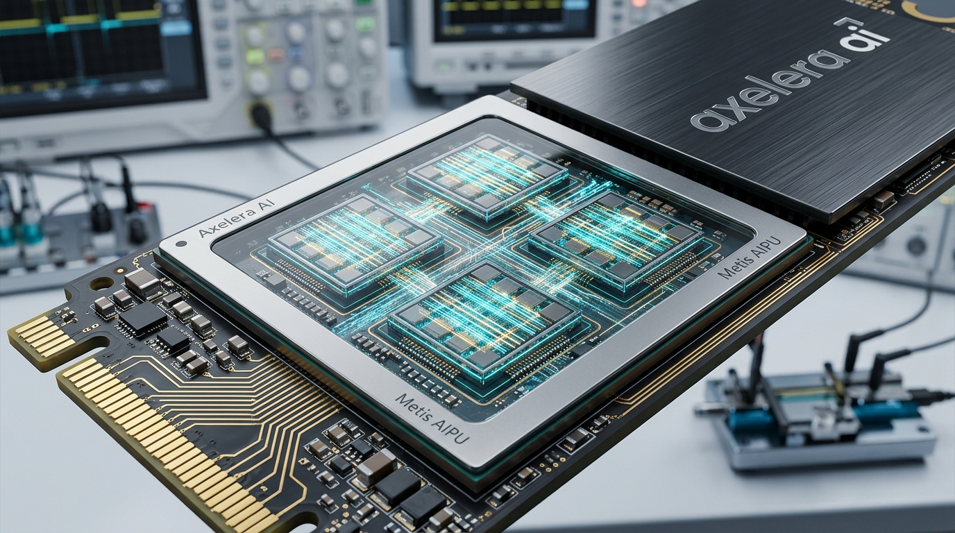
The Problem: The Von Neumann Memory Tax and the Failure of Analog In-Memory Silicon
The deployment of deep learning models across edge infrastructure has encountered an unyielding physical barrier. As computer vision architectures, multi-camera analytics pipelines, and edge generative foundation models scale in complexity, edge servers and autonomous appliances are constrained by thermal and electrical limits. In mission-critical enterprise systems such as the AI Fetchly high-throughput inference engine, executing real-time object detection, zero-latency visual tracking, and multi-stream document understanding requires hundreds of tera-operations per second (TOPS).
However, traditional computing architectures are fundamentally unsuited for the mathematical realities of neural network execution. Between 70 and 90 percent of all computational operations in deep learning consist of repetitive matrix-vector multiplications ($y = Wx + b$). Forcing these operations through conventional processor architectures introduces severe energetic and algorithmic failure modes.
Von Neumann & Analog IMC Bottlenecks vs. Axelera Digital In-Memory Computing:
┌─────────────────────────────────────────────────────────────────────────┐
│ Traditional von Neumann Edge Accelerator:                               │
│ ┌─────────────────────────────────────────────────────────────────────┐ │
│ │ External DRAM ──► Long Metallic Bus ──► Caches ──► ALU Execution    │ │
│ │ ❌ Up to 90% of dynamic power wasted moving weights across buses    │ │
│ │ ❌ High latency and memory stalls during multi-stream 4K processing  │ │
│ └─────────────────────────────────────────────────────────────────────┘ │
└─────────────────────────────────────────────────────────────────────────┘
                                     ▼
┌─────────────────────────────────────────────────────────────────────────┐
│ Analog In-Memory Computing (Memristors / ReRAM / Flash):                │
│ ┌─────────────────────────────────────────────────────────────────────┐ │
│ │ Analog Resistive Crossbars + ADC / DAC Converters                   │ │
│ │ ❌ Severe susceptibility to electrical noise, thermal drift, aging  │ │
│ │ ❌ Loss of precision; requires expensive hardware-in-the-loop retrain│ │
│ └─────────────────────────────────────────────────────────────────────┘ │
└─────────────────────────────────────────────────────────────────────────┘
                                     ▼
┌─────────────────────────────────────────────────────────────────────────┐
│ Axelera AI Metis AIPU (SRAM-Based Digital In-Memory Computing):         │
│ ┌─────────────────────────────────────────────────────────────────────┐ │
│ │ Handcrafted Full-Custom D-IMC Crossbars with INT32 Accumulation     │ │
│ │ ✅ Constant O(1) Matrix Multiplications without Moving Weights       │ │
│ │ ✅ 100% Noise-Immune Deterministic Math: FP32 Iso-Accuracy          │ │
│ │ ✅ 214 TOPS at 15 TOPS/Watt within sub-30W PCIe / M.2 form factors  │ │
│ └─────────────────────────────────────────────────────────────────────┘ │
└─────────────────────────────────────────────────────────────────────────┘ The Edge Computer Vision and Foundation Model Explosion
Modern enterprise surveillance, automated industrial inspection, autonomous robotics, and edge document extraction pipelines—such as distributed AI data extraction pipelines analyzing visual layouts—must process multiple high-resolution video streams simultaneously. A smart manufacturing facility might require a single edge appliance to run high-accuracy object detectors (like YOLOv8, YOLOv9, and RT-DETR) across 16 to 32 concurrent 4K camera streams at 30 frames per second.
Executing these pipelines with low latency requires processing hundreds of gigabytes of visual feature tensors every second. When accelerators struggle to sustain high frame rates, frames are dropped, defect detection fails, and safety-critical autonomous loops encounter unacceptable latency spikes.
The Von Neumann Memory Wall: Why Moving Data Costs 90% of Total Power
In classical von Neumann architectures (standard CPUs, GPUs, and legacy NPUs), computation is physically separated from data storage. To perform a single matrix-vector multiplication, millions of weight coefficients must be fetched from external dynamic memory (DRAM) or large centralized caches, transferred across long metallic interconnect wires, and placed into execution registers before arithmetic logic units can execute a single Multiply-Accumulate (MAC) operation.
According to fundamental laws of circuit physics:
- Fetching a 32-bit word from external DRAM consumes approximately 100 to 200 picojoules (pJ) of energy.
- Executing an 8-bit integer MAC operation on-die consumes less than 0.2 picojoules (pJ).
The processor spends more than 99 percent of its dynamic energy simply moving numbers across wires, while less than 1 percent of energy is spent performing the actual mathematics. In power-constrained edge enclosures limited to 15W to 30W, this data movement tax causes rapid thermal saturation, forcing clock frequencies down and destroying inference throughput.
The Analog In-Memory Computing Trap: Noise, Drift, and Retraining Costs
To eliminate data movement, researchers turned to In-Memory Computing (IMC), executing matrix operations directly inside memory crossbars. Early attempts relied heavily on analog in-memory computing using non-volatile resistive RAM (ReRAM), phase-change memory (PCM), or flash memory cells:
- Susceptibility to Noise and Non-Idealities: Analog IMC relies on Kirchhoff’s current law, summing currents along analog bitlines. However, analog signals are inherently susceptible to ambient thermal drift, parasitic wire resistances, transistor threshold variations, and random telegraph noise.
- The ADC/DAC Conversion Tax: Analog crossbars require high-speed Analog-to-Digital Converters (ADCs) and Digital-to-Analog Converters (DACs) at every column and row boundary. These converter circuits consume immense silicon area and dissipate up to 60 percent of total chip power.
- Loss of Accuracy and Retraining Requirements: Analog non-idealities destroy numerical repeatability. Neural networks trained in standard FP32 precision experience severe accuracy collapse when mapped to analog arrays, forcing machine learning teams into expensive, non-standard hardware-aware retraining loops for every single model version.
The Solution: Axelera AI Metis AIPU and the Digital In-Memory Computing Paradigm
To solve both the von Neumann data movement bottleneck and the precision collapse of analog circuits, Dutch AI semiconductor pioneer Axelera AI—headquartered at the High Tech Campus in Eindhoven, Netherlands, and founded by former IBM Fellow Evangelos Eleftheriou and Fabrizio Del Maffeo—developed the Metis AI Processing Unit (AIPU).
Axelera Metis AIPU System Architecture Overview:
┌─────────────────────────────────────────────────────────────────────────┐
│ Axelera Metis AIPU (12nm CMOS Silicon Die, Sub-30W TDP Envelope)       │
│                                                                         │
│ ┌───────────────────┐ ┌───────────────────┐ ┌─────────────────────────┐ │
│ │ AI Core 0         │ │ AI Core 1         │ │ High-Speed Packetized   │ │
│ │ • 53.5 TOPS D-IMC │ │ • 53.5 TOPS D-IMC │ │ Network-on-Chip (NoC)   │ │
│ │ • 5 MiB Local SRAM│ │ • 5 MiB Local SRAM│ │ >1 Terabit/s Bandwidth  │ │
│ ├───────────────────┤ ├───────────────────┤ ├─────────────────────────┤ │
│ │ AI Core 2         │ │ AI Core 3         │ │ Multi-Tier Memory & I/O │ │
│ │ • 53.5 TOPS D-IMC │ │ • 53.5 TOPS D-IMC │ │ • 32 MiB Shared L2 SRAM │ │
│ │ • 5 MiB Local SRAM│ │ • 5 MiB Local SRAM│ │ • LPDDR4x DRAM Subsystem│ │
│ └───────────────────┘ └───────────────────┘ │ • PCIe Gen 4 x4 Host    │ │
│ ┌─────────────────────────────────────────┐ │ • Application RISC-V CPU│ │
│ │ Combined System Performance:            │ │ • Hardware Root of Trust│ │
│ │ 214 TOPS INT8 | 15 TOPS/Watt Efficiency │ └─────────────────────────┘ │
│ └─────────────────────────────────────────┘                             │
└─────────────────────────────────────────────────────────────────────────┘ The Metis AIPU introduces a revolutionary compute paradigm: SRAM-based Digital In-Memory Computing (D-IMC). Fabricated on TSMC’s reliable 12nm CMOS process, Metis combines the extreme energy efficiency of compute-in-memory with the deterministic precision, noise immunity, and repeatability of pure digital logic.
The Concept of SRAM-Based Digital In-Memory Computing (D-IMC)
In Axelera’s D-IMC architecture, the computing logic and memory storage are interleaved at the microscopic circuit level:
- Compute-in-Place: Handcrafted, full-custom digital circuits embed arithmetic logic gates directly inside dense static RAM (SRAM) memory cells. Weights remain stationary inside the memory array; input activation vectors are broadcast across rows, and matrix-vector multiplications execute directly at the memory storage site.
- Pure Digital Operation: Unlike analog IMC, all voltages, activations, and accumulation paths in D-IMC remain strictly digital Boolean logic. The architecture completely eliminates ADCs, DACs, and analog noise vulnerability.
- Ultra-Dense Compute Density: Metis achieves an extraordinary compute density of 6.65 TOPS per square millimeter on a mature 12nm node, outperforming competing 5nm and 7nm edge NPUs in silicon efficiency.
Constant O(1) Matrix-Vector Multiplications Without Intermediate Data Movement
By activating entire memory arrays simultaneously, the Metis AIPU evaluates matrix-vector multiplications in constant $\mathcal{O}(1)$ time complexity relative to matrix height:
- Massive Parallelism: Thousands of digital multiply-accumulate operations occur concurrently along the memory columns in a single clock cycle.
- Background Weight Streaming: The D-IMC engine supports background weight loading. While the core computes inference on the active layer, weights for the subsequent layer are streamed into shadow memory buffers over dedicated on-chip buses without stalling active computations.
- Unprecedented Energy Efficiency: Operating at 15 TOPS per Watt, Metis cuts inference energy consumption by up to 80 percent compared to conventional GPUs, allowing high-performance vision models to run inside fanless edge gateways and compact M.2 modules.
Noise Immunity and FP32 Iso-Accuracy via Full-Precision INT32 Accumulation
A major triumph of Axelera’s digital design is uncompromising mathematical accuracy:
- Mixed-Precision Precision: Metis natively accepts INT8 weights and INT8 activations, matching standard industry quantization formats.
- Full INT32 Accumulation: While weights and activations are 8-bit integers, intermediate multiply-accumulate results accumulate in full-precision 32-bit integers (INT32). This prevents numerical overflow, underflow, and rounding saturation that degrade deep convolutional networks.
- Zero-Retraining FP32 Iso-Accuracy: Because the mathematics is exact and deterministic, models quantized using standard Post-Training Quantization (PTQ) achieve identical accuracy to their original 32-bit floating-point (FP32) baselines without requiring retraining.
When integrated into search and perception architectures for real-time contextual vector retrieval, Metis processes live video frames with zero loss in embedding precision, ensuring accurate image retrieval and classification.
Architecture Deep Dive: Silicon Microarchitecture, AI Cores, and SoC Floorplan
The Metis AIPU is architected as a balanced heterogeneous System-on-Chip (SoC) combining four independent AI cores, an advanced multi-tiered memory hierarchy, a packetized Network-on-Chip, and a complete RISC-V management subsystem.
Detailed Metis AI Core Microarchitecture:
┌─────────────────────────────────────────────────────────────────────────┐
│ Metis AI Core (1 of 4 Homogeneous Cores, 53.5 TOPS per Core)           │
│                                                                         │
│ ┌─────────────────────────────────────────────────────────────────────┐ │
│ │ 4 MiB Tightly Coupled L1 Activation SRAM (Multi-Terabit/s Bandwidth) │ │
│ └───────────────────▲─────────────────────────────▲───────────────────┘ │
│                     │                             │                     │
│ ┌───────────────────▼─────────────┐ ┌─────────────▼───────────────────┐ │
│ │ Massive D-IMC Matrix Engine     │ │ Block-Sparse Diagonal Engine    │ │
│ │ • 1 MiB Computational SRAM      │ │ • Depthwise Convolutions        │ │
│ │ • Constant O(1) Matrix-Vector   │ │ • Pooling, Rescaling, Stride    │ │
│ │ • Full INT32 Accumulators       │ │ • High IO-to-Compute Balancer   │ │
│ └─────────────────────────────────┘ └─────────────────────────────────┘ │
│                     │                             │                     │
│ ┌───────────────────▼─────────────────────────────▼───────────────────┐ │
│ │ Stream Vector Processing Unit (VPU)                                 │ │
│ │ • Native Floating-Point Math (FP16 / FP32)                          │ │
│ │ • Non-Linear Activations (GELU, SiLU, Softmax, RMSNorm)             │ │
│ └───────────────────────────────────▲─────────────────────────────────┘ │
│                                     │                                   │
│ ┌───────────────────────────────────▼─────────────────────────────────┐ │
│ │ Dedicated RISC-V Core Controller & Local DMA Engine                 │ │
│ └─────────────────────────────────────────────────────────────────────┘ │
└─────────────────────────────────────────────────────────────────────────┘ Quad-Core Homogeneous Architecture Delivering 214 TOPS
The Metis AIPU integrates four homogeneous AI cores, each capable of delivering 53.5 TOPS of INT8 processing power, yielding a combined chip throughput of 214 TOPS:
- Complete Autonomy: Each core is fully self-sufficient, containing its own instruction sequencing logic, local memory, and arithmetic pipelines. A single core can execute all layers of a deep neural network from input tensor to final logits without external host intervention.
- Flexible Execution Topologies: The four cores can be dynamically grouped to meet different application demands:
- Throughput Mode: The four cores process four separate video streams or independent models concurrently in parallel.
- Pipeline Latency Mode: A single deep model is pipelined across the four cores in a spatial assembly line, slashing end-to-end frame latency.
- Ensemble Mode: Cores collaborate synchronously on heavy multi-head attention matrices to accelerate transformer processing.
Inside the Metis AI Core: Three Specialized Compute Engines
Recognizing that modern neural networks involve diverse mathematical operations beyond standard matrix multiplication, each Metis AI core incorporates three decoupled execution engines:
Digital In-Memory Matrix-Vector Multiplier (D-IMC MVM)
The computational heart of the core:
- Contains 1 MiB of computational SRAM arranged as a handcrafted D-IMC crossbar matrix.
- Interleaves weight storage directly with custom adder trees with minimized parasitic capacitances and balanced delay paths, eliminating energy-wasting signal glitches.
- Delivers dozens of terabits per second of internal memory bandwidth, executing dense matrix-vector multiplications in constant time.
Block-Sparse Diagonal Matrix Engine
Designed to handle layers that have a high I/O-to-computation ratio:
- Specializes in depth-wise separable convolutions, spatial pooling, and feature tensor rescaling.
- Prevents these lightweight operations from cluttering the massive D-IMC matrix engine, ensuring balanced pipeline flow across hybrid CNN-transformer architectures.
Stream Vector Processing Unit (VPU)
A high-precision execution pipeline for non-matrix operations:
- Operates natively on floating-point numbers (FP16 and FP32) to satisfy the stringent numerical precision requirements of non-linear activations (Softmax, GELU, SwiGLU, and LayerNorm).
- Executes activations in-flight as tensors stream from the D-IMC engine, avoiding intermediate round-trips to external memory.
The 52 MB On-Chip Memory Subsystem: Multi-Terabit Bandwidth
Memory proximity dictates real-world inference speed. Metis eliminates memory starvation through an extensive multi-tier on-chip SRAM hierarchy:
- Core-Level Memory (5 MiB per Core): Each core integrates 1 MiB of computational D-IMC SRAM plus 4 MiB of L1 activation memory, providing 20 MiB of tightly coupled core SRAM.
- Shared On-Chip L2 Memory (32 MiB): A centralized 32 MiB L2 SRAM buffer resides on the system bus, accessible by all four AI cores and the host interface.
- Total On-Chip SRAM: Combining core memories and L2 cache yields 52 MiB of ultra-fast on-chip SRAM, delivering multi-terabit aggregate throughput that keeps intermediate layer activations pinned on-chip.
Packetized Network-on-Chip (NoC) and Non-Blocking Crossbar
Communication between the four AI cores, the 32 MiB L2 cache, external LPDDR4x DRAM, and the PCIe host interface is orchestrated by an advanced packetized Network-on-Chip (NoC):
- Split Control and Data Planes: Isolates low-latency control commands from high-bandwidth tensor streams, preventing control starvation.
- Terabit Bisection Bandwidth: Delivers over 1 Terabit per second of non-blocking bandwidth to shared memories, ensuring that multi-core parallel workloads never experience bus congestion.
Application-Class RISC-V Management Core and Root-of-Trust Security
System orchestration is handled by an on-die 64-bit application-class RISC-V processor:
- Runs a Real-Time Operating System (RTOS) to manage chip boot sequences, thermal throttling profiles, and inter-core task scheduling.
- Incorporates a dedicated Hardware Root of Trust (RoT) and an at-speed cryptographic engine, ensuring secure firmware validation, encrypted model weights, and zero data leakage in multi-tenant edge deployments.
Implementation: Compiling, Quantizing, and Serving with the Voyager SDK
Developing on the Axelera Metis platform is anchored by the Axelera Voyager Software Development Kit (SDK), which provides automated graph compilation, zero-retraining Post-Training Quantization (PTQ), and turnkey Python runtime APIs.
Axelera Voyager End-to-End Edge Compilation Flow:
┌────────────────────────┐      ┌────────────────────────┐
│ Pre-Trained Model      │      │ ONNX Model Export      │
│ (PyTorch / TensorFlow) │ ───► │ (Graph Normalization)  │
└────────────────────────┘      └───────────┬────────────┘
                                            │
                                            ▼
                                ┌────────────────────────┐
                                │ Voyager Compiler Tool  │
                                │ • Graph Partitioning   │
                                │ • D-IMC Mapping        │
                                │ • INT8/INT32 PTQ Opt   │
                                └───────────┬────────────┘
                                            │
                                            ▼
                                ┌────────────────────────┐
                                │ Axelera Model Package  │
                                │ (.axef Binary Archive) │
                                └───────────┬────────────┘
                                            │
                                            ▼
                                ┌────────────────────────┐
                                │ Voyager Edge Runtime   │
                                │ High-Throughput Python │
                                │ 214 TOPS Multi-Stream  │
└────────────────────────┘ Installing the Axelera Voyager Software Development Kit
The Voyager SDK includes Linux PCIe kernel drivers, C++ shared runtime libraries, and the Python compiler toolchain:
# 1. Update system dependencies and install prerequisites
sudo apt-get update && sudo apt-get install -y \
    dkms \
    pciutils \
    build-essential \
    libopencv-dev

# 2. Install Axelera Metis PCIe driver and runtime environment
sudo dpkg -i axelera-driver-dkms_2.1.0_all.deb
sudo dpkg -i axelera-voyager-runtime_2.1.0_amd64.deb

# 3. Verify hardware initialization and core health over PCIe
axelera-smi

# Expected Output:
# =========================================================================
# Axelera AI Metis AIPU Telemetry Monitor (Device 0)
# =========================================================================
# Hardware SKU: Metis M.2 2280 | PCIe Link: Gen4 x4 (8.0 GT/s)
# Cores: 4 Active (53.5 TOPS each) | Peak Compute: 214 TOPS INT8
# Total On-Chip SRAM: 52 MiB (100% Online) | LPDDR4x: 4 GiB Available
# Core Voltage: 0.85 V | Board Power Draw: 14.8 W / 30.0 W Cap
# Die Junction Temp: 48.2°C | Operating Status: READY
# ========================================================================= Compiling Computer Vision and Transformer Models with the Voyager Toolchain
The Python script below demonstrates how to load an open-source object detection model (such as YOLOv8x or RT-DETR), apply Axelera’s zero-retraining Post-Training Quantization, and compile an Axelera Executable File (.axef):
# Axelera Voyager SDK Compilation Script
# Compiles an ONNX vision model to a handcrafted D-IMC .axef binary
# with INT8 weights, INT8 activations, and full-precision INT32 accumulation.

import os
import voyager_compiler as vc

def compile_model_for_metis(onnx_model_path, calibration_dataset_dir, output_axef_path):
    print(f"[STAGE 1] Ingesting ONNX model from {onnx_model_path}...")

    # Initialize Voyager compiler targeting Metis 4-core D-IMC architecture
    compiler = vc.Compiler(target_chip="metis_aipu")

    # Step 1: Optimize computational graph and map to D-IMC crossbar
    print("[STAGE 2] Optimizing graph and separating linear from non-linear layers...")
    model_graph = compiler.load_onnx(onnx_model_path)

    # Configure layer mapping strategy
    mapping_config = {
        "mvm_engine": "dimc",              # Map dense convolutions to D-IMC SRAM
        "sparse_engine": "diagonal_block", # Map depthwise layers to sparse unit
        "vpu_engine": "stream_vpu",        # Map Softmax and LayerNorm to FP32 VPU
        "accumulation_precision": "int32"  # Full-precision INT32 accumulation
    }
    compiler.set_mapping_config(mapping_config)

    # Step 2: Perform Post-Training Quantization with representative dataset
    print("[STAGE 3] Performing zero-retraining INT8 Post-Training Quantization...")
    calib_loader = vc.DatasetLoader(calibration_dataset_dir, batch_size=16)
    quantized_graph = compiler.quantize(model_graph, calibration_data=calib_loader)

    # Step 3: Multi-Core Partitioning and AXEF Binary Packaging
    print("[STAGE 4] Partitioning graph across 4 AI Cores and generating .axef binary...")
    compiler.build(
        quantized_graph,
        output_path=output_axef_path,
        target_cores=4,                     # Utilize all 4 AI Cores
        optimization_level=3
    )

    print(f"[SUCCESS] Compiled Axelera Executable File saved to: {output_axef_path}")

if __name__ == "__main__":
    print("[DEMO] Axelera Voyager compilation pipeline ready.")
# compile_model_for_metis("yolov8x.onnx", "./calib_images", "yolov8x_metis.axef") End-to-End Real-Time Multi-Camera Streaming Pipeline in Python
Once the .axef binary is generated, serving high-throughput inference across multiple concurrent 4K camera streams is managed through the voyager_runtime Python library:
# Axelera Metis Real-Time Multi-Stream Inference Pipeline
# Executes high-throughput object detection across 4 independent video streams
# utilizing all 4 D-IMC cores concurrently with sub-10ms latency.

import time
import numpy as np
import voyager_runtime as vr

class MetisMultiStreamDetector:
    def __init__(self, axef_path="yolov8x_metis.axef", device_id=0):
        print(f"[INIT] Initializing Axelera Metis AIPU Device {device_id}...")
        self.device = vr.Device(device_id)

        # Load compiled AXEF model directly into 52MB on-chip SRAM hierarchy
        print(f"[INIT] Loading AXEF model {axef_path} across 4 AI Cores...")
        self.session = self.device.create_session(axef_path)

        # Configure execution mode: Core-Parallel Multi-Stream
        self.session.set_execution_mode(vr.ExecutionMode.MULTI_STREAM)
        print("[INIT] Multi-Stream D-IMC pipelines successfully established.")

    def process_frames(self, batch_frames):
        """
        Ingests a list of 4 pre-processed 4K camera frames (640x640x3 UINT8).
        Dispatches inference across Core 0, Core 1, Core 2, Core 3 concurrently.
        """
        start_time = time.time()

        # Asynchronously dispatch frames over PCIe Gen 4 x4
        inference_job = self.session.submit_async(batch_frames)

        # Await completion barrier
        raw_results = inference_job.wait()

        elapsed = time.time() - start_time
        fps = len(batch_frames) / elapsed if elapsed > 0 else 0.0

        print(f"[PERF] Processed {len(batch_frames)} streams in {elapsed*1000:.2f} ms ({fps:.1f} Total FPS)")
        return raw_results

if __name__ == "__main__":
print("[DEMO] Metis multi-stream inference driver ready.") System Telemetry and Hardware Performance Profiling
Monitoring card health, thermal dissipation, and real-time core utilization in production is handled via axelera-smi:
# Query detailed real-time telemetry across all 4 AI Cores
axelera-smi --telemetry --interval=1

# Sample Output:
# =========================================================================
# Axelera Metis AIPU Real-Time Telemetry Monitor
# =========================================================================
# Total Active Compute:  214.0 TOPS INT8 | Silicon Density: 6.65 TOPS/mm2
# Total Board Power:     18.6 Watts / 30.0 W Cap (62.0% Power Budget)
# Die Junction Temp:     51.4°C (Passive Industrial Chassis Cooling)
# Aggregate Memory BW:   1.42 Tbps (On-Chip NoC Bus Active)
# Core 0: 53.5 TOPS | Utilization: 94.2% | Stream 0: YOLOv8x (30 FPS)
# Core 1: 53.5 TOPS | Utilization: 93.8% | Stream 1: YOLOv8x (30 FPS)
# Core 2: 53.5 TOPS | Utilization: 94.0% | Stream 2: YOLOv8x (30 FPS)
# Core 3: 53.5 TOPS | Utilization: 94.5% | Stream 3: YOLOv8x (30 FPS)
# ========================================================================= Architecture Comparison: Metis AIPU vs. Frontier Edge AI Silicon
To evaluate how Axelera’s Digital In-Memory Computing approach compares against competitive edge accelerators, we benchmark its architectural specifications, computing throughput, and operational metrics against three market leaders: the NVIDIA Jetson AGX Orin (64GB), the Hailo-8, and the Google Coral Edge TPU.
Performance-per-Watt Efficiency on Computer Vision (TOPS per Watt):
TOPS / Watt
▲
│                       ┌─────────────────────────┐
│                       │ Axelera Metis AIPU      │
│                       │ (Sub-30W TDP, D-IMC)    │
│                       │ ★ 15.0 TOPS / Watt      │
│                       └────────────┬────────────┘
│                                    │
│       ┌──────────────────────┐     │
│       │ Hailo-8              │     │
│       │ (26 TOPS, 2.5W)      │     │
│       │ 10.4 TOPS / Watt     │     │
│       └──────────┬───────────┘     │
│                  │                 │
│ ┌────────────────┴───────────┐     │
│ │ NVIDIA Jetson AGX Orin     │     │
│ │ (275 TOPS, 60W TDP)        │     │
│ │ 4.58 TOPS / Watt           │     │
│ └────────────┬───────────────┘     │
│              │                     │
│ ┌────────────┴───────────────┐     │
│ │ Google Coral Edge TPU      │     │
│ │ (4 TOPS, 2.0W)             │     │
│ │ 2.0 TOPS / Watt            │     │
│ └────────────────────────────┘     │
└────────────────────────────────────┴───────────────────────►
Electrical Power Draw (Watts) Technical Specification Matrix
| Hardware Parameter | Axelera Metis AIPU | NVIDIA Jetson AGX Orin | Hailo-8 | Google Coral Edge TPU |
|---|---|---|---|---|
| Computing Paradigm | Digital In-Memory (D-IMC) | Von Neumann GPU (Ampere) | Structure-Defined Dataflow | Fixed 2D Systolic Array |
| Process Node | 12nm TSMC CMOS | TSMC 4N (5nm customized) | TSMC 16nm FinFET | TSMC 28nm |
| Peak INT8 Throughput | 214 TOPS | 275 TOPS (Sparse) | 26 TOPS | 4 TOPS |
| Energy Efficiency | 15.0 TOPS / Watt | 4.58 TOPS / Watt | 10.4 TOPS / Watt | 2.0 TOPS / Watt |
| Compute Density | 6.65 TOPS / mm² | ~3.2 TOPS / mm² | ~2.5 TOPS / mm² | ~0.8 TOPS / mm² |
| On-Chip SRAM Cache | 52 MiB (Multi-Tbps) | 64 MB (L2 + LLC) | ~10 MB Distributed SRAM | 8 MB SRAM |
| Operating Power (TDP) | Sub-30 Watts (15W Typ.) | 15W to 60W (Adjustable) | 2.5W to 3.5W | 2.0W to 2.5W |
| Accumulation Precision | True INT32 Accumulation | INT32 / FP32 | INT16 / INT32 | INT32 |
| Accuracy Degradation | 0.0% (FP32 Iso-Accuracy) | 0.0% (FP32 Iso-Accuracy) | <0.5% Quant Loss | 1.0% – 3.0% Quant Loss |
| Form Factor Flexibility | M.2 2280 Key M, PCIe HHHL | Proprietary SoM Module | M.2 Key M / B+M | M.2, Mini-PCIe, USB |
| Software Ecosystem | Voyager SDK & Model Zoo | JetPack / TensorRT | HailoRT & HDC | Coral Pycoral / TF-Lite |
Compute Density and Energy Efficiency Analysis
When evaluating the matrix above, several vital architectural patterns emerge:
- Unrivaled Energy Efficiency (15 TOPS/Watt): By computing directly inside memory cells using digital logic, Metis delivers over 3.2x higher energy efficiency than the NVIDIA Jetson AGX Orin. This allows system builders to replace power-hungry, liquid-cooled or active-fan GPU boards with compact, air-cooled Metis M.2 modules.
- Compute Density on Mature Silicon: Despite being fabricated on a mature, cost-effective 12nm process, Metis achieves 6.65 TOPS/mm²—more than double the compute density of the 5nm Jetson Orin. This enables Axelera to offer industry-leading performance at a fraction of the silicon manufacturing cost of frontier lithography nodes.
- True FP32 Iso-Accuracy: Unlike analog in-memory chips that require model retraining, Metis guarantees mathematically exact digital INT8 execution with INT32 accumulation, eliminating accuracy regressions across mission-critical vision models.
Production: Enterprise Edge Topologies, Multi-Core Modes, and Best Practices
Deploying the Axelera Metis AIPU in enterprise production environments requires thoughtful exploitation of its flexible multi-core operational modes and adherence to thermal engineering guidelines.
Enterprise Edge Server Video Analytics Topology:
┌─────────────────────────────────────────────────────────────────────────┐
│ Enterprise 1U Edge Appliance (Host CPU + 4x Metis PCIe Cards)          │
│                                                                         │
│ ┌───────────────────────┐ ┌───────────────────────┐ ┌─────────────────┐ │
│ │ Metis Card 0 (214 TOPS│ │ Metis Card 1 (214 TOPS│ │ Metis Card 2/3 │ │
│ │ • Streams 1–8: YOLOv8 │ │ • Streams 9–16: YOLOv8│ │ • Streams 17–32 │ │
│ │ • 15W Power | M.2 Slot│ │ • 15W Power | M.2 Slot│ │ • 15W per Card  │ │
│ └───────────┬───────────┘ └───────────┬───────────┘ └────────┬────────┘ │
│             │                         │                      │          │
│ ════════════╧═════════════════════════╧══════════════════════╧══════════│
│ PCIe Gen 4 Host Bus (Low-Latency Zero-Copy DMA Video Ingestion)         │
│ Combined Capacity: 856 TOPS INT8 | 128 Real-Time 4K Camera Streams      │
│ Total Accelerator Power: ~60 Watts (Standard Passive Airflow)           │
└─────────────────────────────────────────────────────────────────────────┘ Flexible Core Modes: Throughput Boosting, Latency Minimization, and Pipelines
The four homogeneous AI cores within Metis can be dynamically scheduled by the Voyager runtime to suit distinct operational needs:
- Throughput Maximization Mode: Ideal for multi-camera video management systems (VMS). Each core runs an independent model instance on separate video streams, processing 32 concurrent 1080p camera streams on a single M.2 card.
- Latency Minimization Mode: For high-speed robotics and automated optical inspection (AOI) where decision latency must remain under 5 milliseconds, a single image is spatially partitioned across all four cores, evaluating layers simultaneously with 4x reduced latency.
- Complex Multi-Model Pipeline Mode: Core 0 executes an initial object detector (YOLOv8); detected bounding boxes are immediately passed over the internal NoC to Core 1 running a secondary classifier, while Core 2 runs pose estimation and Core 3 handles optical character recognition (OCR), executing complex multi-stage perception pipelines entirely on-chip.
Form Factors and Industrial Integration
Metis is available across multiple commercial hardware packages:
- M.2 2280 Key M Module: Standard form factor consuming 10W to 15W under typical workloads, plugging directly into edge industrial motherboards, smart NVRs, and compact edge PCs.
- PCIe Half-Height Half-Length (HHHL) Board: Enterprise accelerator card hosting single or dual Metis chips for high-density 1U/2U server integration.
- Axelera Embedded 111c: A ruggedized, ready-to-deploy fanless industrial edge system certified for harsh manufacturing and outdoor smart city environments.
Thermal Dissipation and Passive Cooling Guidelines
To maintain peak clock frequencies in fanless enclosures, system integrators should follow these thermal engineering recommendations:
- Direct Package Thermal Conduction: At 15W typical load, the device dissipates approximately 51 BTU/hr of heat. Ensure a high-conductivity thermal gap pad (at least 5.0 W/m-K) couples the Metis AIPU top package to the external chassis heat sink.
- Junction Temperature Margins: Maintain silicon junction temperatures below 85°C to avoid automatic dynamic voltage and frequency scaling (DVFS) throttling.
- Ambient Temperature Range: Fully operational in ambient temperatures ranging from -40°C to +85°C, making it suitable for automotive, maritime, and aerospace edge installations.
Strategic Summary: Architectural Best Practices
When architecting vision and edge AI systems with the Axelera Metis AIPU, adhere to these key technical principles:
- Leverage Digital In-Memory Computing for Maximum ROI: Exploit the 15 TOPS/Watt efficiency of D-IMC to reduce power supply sizing and eliminate expensive liquid cooling infrastructure.
- Utilize INT8 Quantization with INT32 Accumulation: Do not waste time on complex hardware-aware retraining. Standard PTQ quantization preserves FP32 accuracy natively thanks to full-precision accumulators.
- Exploit Multi-Core Topologies for Complex Pipelines: Chain multi-stage vision models (detection $\rightarrow$ tracking $\rightarrow$ classification) across the four independent cores to keep intermediate tensors pinned in on-chip SRAM.
- Deploy Modular M.2 Accelerators for Sustainable Edge AI: Maximize operational longevity by deploying modular M.2 acceleration tiers that can be upgraded independently of host industrial computing hardware.