AMD Instinct MI300X Guide: CDNA 3 & 192GB LLM Serving
The Memory Capacity Wall in Modern Enterprise AI Serving
In modern enterprise foundation model serving, low-latency agent copilots, and autonomous data intelligence systems powered by AI Fetchly, computational infrastructure is governed by a fundamental physical constraint: the Memory Capacity and Bandwidth Wall. Whether executing real-time data ingestion pipelines via real-time data ingestion, parsing thousands of unstructured web documents with automated web scraping, or streaming reasoning tokens from frontier models, GPU memory limitations dictate infrastructure economics.
Over the past three years, the parameter scale and context lengths of Large Language Models (LLMs) have expanded at a rate that vastly outpaces semiconductor memory scaling. While models have scaled from 7 billion to 70 billion and 405 billion parameters (such as the LLaMA-3.1 and LLaMA-3.3 series), standard datacenter GPUs remained capped at 80 GB of High-Bandwidth Memory (HBM) for multiple hardware generations.
This disparity creates severe systemic bottlenecks for enterprise software engineering and infrastructure teams:
1. The Mandatory Tensor Parallelism Tax
Serving a state-of-the-art 70B parameter foundation model in 16-bit precision (FP16 or BF16) requires approximately 140 GB of raw memory just to store model weights:
$$\text{Weight Memory} = 70 \times 10^9 \times 2 \text{ bytes} \approx 140 \text{ GB}$$
When factoring in the dynamic Key-Value (KV) cache for extended context windows (e.g., 8k to 128k tokens) and activation buffers, serving LLaMA-3-70B demands a minimum of 160 GB to 180 GB of high-speed memory.
On conventional 80 GB accelerators (such as the NVIDIA A100 or H100 SXM5), fitting a 70B model onto a single GPU is physically impossible. Engineering teams are forced to shard the model across multiple GPUs using Tensor Parallelism (TP):
- Sharding across two 80 GB GPUs ($TP = 2$) leaves virtually zero residual memory headroom for KV cache buffers, limiting concurrency to batch sizes of 1 or 2 before running out of memory (OOM).
- Sharding across four GPUs ($TP = 4$) consumes four expensive accelerator sockets, driving up cloud infrastructure expenditures.
- Crucially, Tensor Parallelism requires cross-GPU synchronization barriers (all-reduce communications) at every single transformer attention and MLP layer. In an 80-layer model, each generated token requires 160 blocking inter-GPU network exchanges.
- These continuous all-reduce operations saturate high-speed links, degrade scaling efficiency, and introduce high tail latencies that cripple real-time conversational user experiences.
- In high-concurrency production deployments, communication overhead can consume up to 40% of the total forward pass execution time, leaving compute units starved for data.
The Tensor Parallelism Dilemma for 70B Model Serving:
+------------------------------------------------------------------------------------+
| CONVENTIONAL 80GB GPU CLUSTER (NVIDIA H100 SXM5 x2, TP=2)                          |
+------------------------------------------------------------------------------------+
| GPU 0 (80 GB HBM3)           <--- All-Reduce Sync (x160/token) ---> GPU 1 (80 GB)  |
| - 70 GB Weights              | High PCIe / NVLink overhead        | - 70 GB Weights |
| - Only 10 GB for KV Cache    | Frequent pipeline bubbles          | - 10 GB KV Cache|
| - Result: Severe concurrency limits; frequent OOMs on long context windows         |
+------------------------------------------------------------------------------------+
| AMD INSTINCT MI300X (SINGLE ACCELERATOR, TP=1)                                     |
+------------------------------------------------------------------------------------+
| Single MI300X GPU (192 GB HBM3, 5.3 TB/s Bandwidth)                                |
| - 140 GB Weights (Full BF16) or 70 GB Weights (FP8)                                |
| - 52 GB to 122 GB Dedicated High-Speed KV Cache Headroom                           |
| - ZERO Inter-GPU All-Reduce Latency; 100% Compute Saturation on Local Matrix Cores |
+------------------------------------------------------------------------------------+ 2. The Context Length Memory Explosion
Modern enterprise applications require models to process immense context prompts: ingesting multi-page financial filings, legal contracts, or entire software repositories. However, the memory footprint of the Key-Value (KV) cache scales linearly with sequence length $S$, batch size $B$, and number of attention layers $L$:
$$\text{KV Cache Memory} = 2 \times 2 \times B \times S \times L \times H_{\text{kv}} \times d_{\text{head}}$$
For a 70B model with grouped-query attention ($H_{\text{kv}} = 8$, $d_{\text{head}} = 128$, $L = 80$):
- At a sequence length of 32,768 tokens, each concurrent user request consumes approximately 5.2 GB of GPU VRAM purely for its KV cache.
- At 64,000 tokens, each stream requires over 10.4 GB of memory.
- On an 80 GB GPU, after loading weights, the remaining memory capacity can serve fewer than 2 concurrent long-context requests before exhausting VRAM.
- Datacenters are forced to throttle concurrency or evict KV blocks, causing latency spikes and degraded throughput.
- When serving autonomous coding agents or recursive multi-turn reasoning loops, the inability to retain large active context pools forces aggressive token truncation, destroying contextual coherence.
3. Supply Chain Monopolies and Enterprise Cloud Costs
The reliance on a single dominant GPU vendor has generated unprecedented economic friction across the technology sector:
- Hyper-scaler cloud providers face multi-quarter hardware allocation backlogs and inflated secondary rental pricing.
- Enterprise developers face soaring compute bills, where running an 8-GPU node of proprietary accelerators costs between $25,000 and $40,000 per month on managed cloud platforms.
- Building competitive AI products requires silicon diversity: high-performance alternative hardware platforms that deliver superior memory capacity, massive memory bandwidth, and an open software ecosystem that breaks proprietary vendor lock-in.
- Vendor lock-in also restricts low-level custom kernel development, as proprietary toolchains guard architectural internals behind closed binary blobs.
The AMD Instinct MI300X Breakthrough
To solve the memory capacity crisis and deliver a high-performance alternative to proprietary GPU architectures, AMD engineered the AMD Instinct MI300X. Built on the AMD CDNA 3 compute architecture, the MI300X is an extraordinary engineering achievement—combining advanced 3D chiplet stacking, massive on-package memory, and an open software stack designed specifically for hyperscale generative AI workloads.
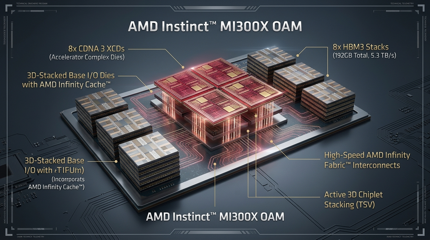
AMD Instinct MI300X Silicon Microarchitecture Schematic:
+------------------------------------------------------------------------------------+
| AMD INSTINCT MI300X ACCELERATOR (TSMC 5nm/6nm 3D Chiplet Package, 750W OAM)        |
+------------------------------------------------------------------------------------+
|                                                                                    |
|  +------------------------------------------------------------------------------+  |
|  | EIGHT CDNA 3 ACCELERATOR COMPLEX DIES (XCDs) - 304 COMPUTE UNITS TOTAL       |  |
|  | - TSMC 5nm Process; 1,216 Matrix Cores (38 CUs per XCD die)                  |  |
|  | - 1,307.4 TFLOPS Dense FP16/BF16 | 2,614.9 TFLOPS Dense FP8 Matrix Compute   |  |
|  +------------------------------------------------------------------------------+  |
|                                        ||                                          |
|               3D Hybrid Die-to-Die Stacking (TSMC SoIC Technology)                 |
|                                        ||                                          |
|  +------------------------------------------------------------------------------+  |
|  | FOUR BASE I/O DIES (IODs) - TSMC 6nm Process                                 |  |
|  | - 256 MB On-Package AMD Infinity Cache (L3 Shared Cache Subsystem)           |  |
|  | - 7x AMD Infinity Fabric 3.0 Links (896 GB/s Bidirectional xGMI Bandwidth)   |  |
|  | - 32-Channel PCIe 5.0 / CXL 2.0 Host Interface Bus                           |  |
|  +------------------------------------------------------------------------------+  |
|                                        ||                                          |
|                2.5D Silicon CoWoS Interposer High-Speed Routing                    |
|                                        ||                                          |
|  +------------------------------------------------------------------------------+  |
|  | EIGHT HBM3 MEMORY DIE STACKS                                                 |  |
|  | - 192 GB Total Capacity (8x 24 GB 12-High HBM3 Stacks)                       |  |
|  | - 5.3 TB/s Peak Theoretical Memory Bandwidth (8,192-bit Interface)           |  |
|  +------------------------------------------------------------------------------+  |
+------------------------------------------------------------------------------------+ 1. 192 GB HBM3: The Single-GPU 70B Paradigm
The defining architectural feature of the AMD Instinct MI300X is its memory subsystem:
- 192 GB of HBM3 Memory: Provides 2.4x the capacity of an 80 GB NVIDIA H100 SXM5 and 1.36x the capacity of a 141 GB H200 SXM.
- 5.3 TB/s Sustained Memory Bandwidth: Delivers 1.6x the memory bandwidth of an H100 (3.35 TB/s) and matches or exceeds cutting-edge memory stacks, driven by an 8,192-bit memory interface across eight 24 GB HBM3 stacks.
- Single-GPU Model Consolidation: With 192 GB of local memory, a single MI300X accelerator hosts an entire LLaMA-3.1-70B model in native BF16 or FP8 on one GPU ($TP = 1$). This completely eliminates cross-GPU tensor communication, slashing generation latency and dramatically simplifying cluster orchestration.
- Massive KV Cache Pool: Because the model fits cleanly on a single board, the remaining ~50 GB of VRAM provides space for over 100,000 active token KV states, enabling unprecedented request concurrency without paging overhead.
2. 153 Billion Transistors Across 12 3D-Stacked Chiplets
Rather than attempting to manufacture an impossibly large monolithic silicon die that would suffer from catastrophic semiconductor yield defects, AMD pioneered advanced 3D chiplet stacking:
- The MI300X integrates 153 billion transistors across 12 active chiplets:
- 8 Accelerator Complex Dies (XCDs): Fabricated on TSMC’s 5nm process node, dedicated strictly to dense mathematical compute.
- 4 Base I/O Dies (IODs): Fabricated on TSMC’s 6nm node, managing memory routing, cache coherency, host PCIe, and interconnects.
- TSMC SoIC (System-on-Integrated-Chips) 3D Hybrid Bonding: The 8 compute dies are vertically bonded directly on top of the 4 I/O dies using copper-to-copper microbumps, achieving phenomenal die-to-die bandwidth density with negligible electrical latency.
- 256 MB of AMD Infinity Cache: Integrated across the base I/O dies, this massive on-package shared L3 cache intercepts repetitive memory accesses, reducing trips to HBM3 and multiplying effective bandwidth.
- Fault-Tolerant Yield Economics: Fabricating smaller individual dies drastically increases wafer yields; any single defective compute die is discarded before packaging, saving thousands of dollars per finished unit.
3. Open Ecosystem via ROCm 6.2 and vLLM
Hardware is only as powerful as the software runtime driving it. With the release of ROCm 6.2 (Radeon Open Compute), AMD has transformed its open-source software stack into a first-class production environment:
- Native integration with frontier inference frameworks: vLLM, SGLang, TensorRT-LLM, and TGI.
- Zero-overhead translation of CUDA code via HIP (Heterogeneous-computing Interface for Portability), allowing engineering teams to compile standard PyTorch CUDA extensions directly for CDNA 3.
- Optimized kernel libraries: Composable Kernel (CK), hipBLASLt, and native ROCm FlashAttention-2 and FlashAttention-3 implementations that achieve near-peak hardware utilization.
- Direct upstream contributions to PyTorch, OpenAI Triton, and vLLM, ensuring that new model architectures (such as DeepSeek-V3 or MoE variants) run on MI300X on day zero.
Deep Dive: CDNA 3 Compute Architecture & 3D Stacking
To understand how the MI300X achieves its computational throughput, we examine the microarchitecture of the CDNA 3 Compute Unit, wavefront scheduling, and the physical chiplet topology.
1. The CDNA 3 Compute Unit (CU) & Matrix Core Engine
The MI300X contains 304 active Compute Units (CUs) distributed evenly across the 8 XCD dies (38 active CUs per die, with 2 additional redundant CUs per die for manufacturing defect tolerance):
- 19,456 Stream Processors (ALUs): Executing general floating-point and integer vector arithmetic.
- 1,216 CDNA 3 Matrix Cores: Dedicated hardware matrix multiplication accelerators that execute Matrix Fused Multiply-Add (MFMA) instructions.
- Dual Wavefront Execution: The compute units support both Wave64 (64 threads executing in lockstep for high-throughput compute) and Wave32 (32 threads for reduced divergence latency in control-flow-heavy kernels).
CDNA 3 Compute Unit (CU) Internal Organization:
+------------------------------------------------------------------------------------+
| CDNA 3 COMPUTE UNIT ARCHITECTURE                                                   |
+------------------------------------------------------------------------------------+
|                                                                                    |
|   +----------------------------------------------------------------------------+   |
|   | 64 KB Local Data Share (LDS) - Shared Memory Scratchpad                    |   |
|   +----------------------------------------------------------------------------+   |
|                                        |                                           |
|   +------------------------------------+---------------------------------------+   |
|   | 4x SIMD16 Vector Execution Units   | 4x CDNA 3 Matrix Core Engines         |   |
|   | - 64 Stream Cores per CU           | - Hardware MFMA Instructions          |   |
|   | - FP32, FP64 Vector Arithmetic     | - FP8, BF16, FP16, TF32, INT8 GEMMs   |   |
|   | - Transcendental Math & Bit Ops    | - 2:4 Structured Sparsity Support     |   |
|   +------------------------------------+---------------------------------------+   |
|                                        |                                           |
|   +----------------------------------------------------------------------------+   |
|   | 32 KB L1 Instruction Cache & 16 KB L1 Scalar Data Cache                    |   |
|   +----------------------------------------------------------------------------+   |
|                                                                                    |
+------------------------------------------------------------------------------------+ 2. Register Files & Matrix Instruction Execution Pipeline
Inside each CDNA 3 Compute Unit, registers are explicitly partitioned between vector processing and matrix accumulation:
- Vector General-Purpose Registers (VGPRs): 256 KB of high-bandwidth register storage per CU, providing operand storage for thread-level operations.
- Accumulator General-Purpose Registers (AGPRs): Dedicated accumulator registers that hold intermediate matrix multiplication results. In CDNA 3, AGPRs can be directly addressed as source operands, eliminating register-copy overhead during multi-step matrix reductions.
- Hardware MFMA Instructions: The Matrix Cores execute hardware instructions like
v_mfma_f32_32x32x16_bf16. In a single instruction issue, 64 threads in a Wave64 block load 16 elements of BFLOAT16 data per thread and compute a complete 32x32 matrix multiplication outer product, accumulating into FP32 registers.
3. Supported Data Precision Formats & Theoretical Performance
The CDNA 3 architecture expands data precision support to encompass all modern AI formats, matching and exceeding datacenter requirements:
| Numeric Precision Format | Dense Peak Throughput | 2:4 Structured Sparsity Throughput | Target AI Workloads |
|---|---|---|---|
| FP8 (E4M3 & E5M2) | 2,614.9 TFLOPS (2.61 PFLOPS) | 5,229.8 TFLOPS (5.23 PFLOPS) | High-throughput LLM Serving & Prefill |
| FP16 / BFLOAT16 | 1,307.4 TFLOPS (1.31 PFLOPS) | 2,614.9 TFLOPS (2.61 PFLOPS) | Foundation Model Pre-training & Fine-tuning |
| INT8 Integer | 2,614.9 TOPS | 5,229.8 TOPS | Quantized Quantization (W8A8) & Vision AI |
| TensorFloat-32 (TF32) | 653.7 TFLOPS | 1,307.4 TFLOPS | Precision Matrix Multiply without code changes |
| FP32 Vector ALUs | 163.4 TFLOPS | N/A | Normalization, Softmax, RoPE Positional Encoding |
| FP64 Double Precision | 81.7 TFLOPS (163.4 Matrix) | N/A | Scientific Computing & HPC Simulations |
4. The 3D SoIC Vertical Stacking Topology and Cache Hierarchy
The physical integration of the MI300X represents the pinnacle of contemporary packaging engineering:
- The 4 Base I/O Dies form an active silicon substrate measuring approximately 1,400 mm² in aggregate area.
- Each IOD contains 64 MB of AMD Infinity Cache (totaling 256 MB on-chip L3), memory controllers for 2 HBM3 stacks, PCIe Gen 5 controllers, and Infinity Fabric crossbar switches.
- The 8 compute dies (XCDs) are vertically mounted on top of the IODs via Through-Silicon Vias (TSVs) with a 9-micron pitch.
- This direct vertical die-to-die connection provides tens of terabytes per second of interconnect bandwidth between the compute units and the Infinity Cache with virtually zero RC wire delay and fraction-of-a-picojoule energy transfer efficiency.
- Around the perimeter of the active base dies sit eight 24 GB HBM3 memory stacks, connected through a passive 2.5D silicon interposer on an organic package substrate measuring 73.5 mm x 78 mm.
Cross-Sectional Physical Layer of AMD Instinct MI300X Packaging:
+------------------------------------------------------------------------------------+
|  [XCD 0] [XCD 1]   [XCD 2] [XCD 3]   [XCD 4] [XCD 5]   [XCD 6] [XCD 7]  (5nm Compute)|
|    ||      ||        ||      ||        ||      ||        ||      ||      (TSVs 9um)  |
|  +----------------+  +----------------+  +----------------+  +----------------+    |
|  | Base IOD 0     |  | Base IOD 1     |  | Base IOD 2     |  | Base IOD 3     |    |
|  | (64MB L3 Cache)|  | (64MB L3 Cache)|  | (64MB L3 Cache)|  | (64MB L3 Cache)|(6nm)|
|  +----------------+  +----------------+  +----------------+  +----------------+    |
|  [HBM3]   [HBM3]       [HBM3]   [HBM3]     [HBM3]   [HBM3]     [HBM3]   [HBM3]     |
|  ==============================================================================    |
|  Silicon Interposer Substrate (TSMC CoWoS 2.5D Packaging Layer)                    |
|  ==============================================================================    |
|  Organic Package Ball Grid Array (OAM Form Factor, 750W Socket)                    |
+------------------------------------------------------------------------------------+ Production Serving Implementation: vLLM on AMD MI300X with ROCm 6.2
To demonstrate the real-world operational power of the AMD Instinct MI300X, we walk through configuring, deploying, and serving frontier language models using vLLM on ROCm 6.2.
1. Launching the ROCm vLLM Production Container
AMD and the open-source vLLM community provide officially maintained, high-performance Docker images built specifically for CDNA 3 hardware:
# ============================================================================
# Script: launch_mi300x_vllm_container.sh
# Description: Initialize ROCm 6.2 environment with GPU devices and shared memory
# ============================================================================

docker run -d --name mi300x-vllm-service --network host --ipc=host --device=/dev/kfd --device=/dev/dri --group-add video --cap-add=SYS_PTRACE --security-opt seccomp=unconfined -v /data/models:/root/.cache/huggingface -v /data/logs:/workspace/logs -e ROCM_PATH=/opt/rocm -e HIP_VISIBLE_DEVICES=0 -e VLLM_ROCM_USE_AITER=1 -e VLLM_USE_TRITON_FLASH_ATTN=1 rocm/vllm:rocm6.2_mi300_ubuntu22.04_py3.10 vllm serve meta-llama/Llama-3.1-70B-Instruct --host 0.0.0.0 --port 8000 --tensor-parallel-size 1 --dtype bfloat16 --gpu-memory-utilization 0.92 --max-model-len 32768 --enable-chunked-prefill --max-num-batched-tokens 8192 Notice the critical argument: --tensor-parallel-size 1. On an 80 GB GPU, running LLaMA-3.1-70B at --tensor-parallel-size 1 instantly results in a fatal Out-Of-Memory CUDA error. On the MI300X, the 192 GB of HBM3 accommodates the entire 140 GB BF16 model weights with over 36 GB of residual VRAM dedicated entirely to the PagedAttention KV cache, enabling deep concurrent batching on a single accelerator.
2. High-Performance Python Client Inference
Below is a production Python script that interacts with the live MI300X vLLM OpenAI-compatible server, utilizing asynchronous requests to benchmark high-throughput token generation:
# ============================================================================
# File: test_mi300x_inference.py
# Description: Async Client Benchmarking Single-GPU 70B Serving on AMD MI300X
# ============================================================================

import asyncio
import time
import httpx

API_URL = "http://localhost:8000/v1/chat/completions"
HEADERS = {"Content-Type": "application/json"}

async def send_inference_request(client: httpx.AsyncClient, request_id: int):
    payload = {
        "model": "meta-llama/Llama-3.1-70B-Instruct",
        "messages": [
            {
                "role": "system",
                "content": "You are an expert AI systems performance architect."
            },
            {
                "role": "user",
                "content": f"Analyze the memory bandwidth implications of 192GB HBM3 on request {request_id}."
            }
        ],
        "max_tokens": 512,
        "temperature": 0.2,
        "stream": False
    }

    start_time = time.perf_counter()
    try:
        response = await client.post(API_URL, json=payload, timeout=60.0)
        response.raise_for_status()
        data = response.json()
        latency = time.perf_counter() - start_time

        usage = data.get("usage", {})
        completion_tokens = usage.get("completion_tokens", 0)
        throughput = completion_tokens / latency if latency > 0 else 0

        print(f"[Req {request_id:02d}] Done | Tokens: {completion_tokens} | "
              f"Latency: {latency:.2f}s | Speed: {throughput:.1f} tok/s")
        return throughput
    except Exception as e:
        print(f"[Req {request_id:02d}] Error: {str(e)}")
        return 0.0

async def main():
    print("Launching concurrent inference benchmarks against AMD Instinct MI300X...")
    async with httpx.AsyncClient(headers=HEADERS) as client:
        tasks = [send_inference_request(client, i) for i in range(16)]
        throughputs = await asyncio.gather(*tasks)

    valid_speeds = [s for s in throughputs if s > 0]
    if valid_speeds:
        avg_speed = sum(valid_speeds) / len(valid_speeds)
        print(f"
Benchmark Complete! Average Throughput per Stream: {avg_speed:.2f} tok/s")

if __name__ == "__main__":
asyncio.run(main()) 3. Writing Native CDNA 3 HIP Kernels with Matrix Cores
For low-level kernel engineers, AMD’s HIP C++ interface allows directly invoking CDNA 3 Matrix Cores using native intrinsics:
// ============================================================================
// File: cdna3_matrix_core_kernel.hip
// Description: Direct invocation of CDNA 3 MFMA instructions on AMD MI300X
// ============================================================================

#include <hip/hip_runtime.h>
#include <hip/hip_fp16.h>
#include <iostream>

// CDNA 3 Matrix Core Intrinsic: 32x32x16 Matrix Multiplication for BFLOAT16
// Computes D = A * B + C on 32x32 tiles across a 64-thread wavefront
__global__ void mfma_gemm_cdna3_kernel(
    const __hip_bfloat16* __restrict__ A,
    const __hip_bfloat16* __restrict__ B,
    float* __restrict__ C,
    int M, int N, int K
) {
    // 64-thread wavefront execution on CDNA 3 Compute Unit
    int tid = threadIdx.x;
    int bid = blockIdx.x;

    // Local registers holding 16-bit inputs and 32-bit accumulators
    typedef __attribute__((__vector_size__(4 * sizeof(float)))) float float4_t;
    typedef __attribute__((__vector_size__(4 * sizeof(short)))) short short4_t;

    short4_t a_val = {0, 0, 0, 0};
    short4_t b_val = {0, 0, 0, 0};
    float4_t c_acc = {0.0f, 0.0f, 0.0f, 0.0f};

    // Built-in AMD CDNA 3 hardware matrix multiply instruction
    // __builtin_amdgcn_mfma_f32_32x32x16_bf16 executes in hardware on Matrix Cores
    c_acc = __builtin_amdgcn_mfma_f32_32x32x16_bf16(
        *(reinterpret_cast<long long*>(&a_val)),
        *(reinterpret_cast<long long*>(&b_val)),
        c_acc,
        0, 0, 0
    );

    // Write back computed tile to global memory
    int out_idx = bid * 64 + tid;
    if (out_idx < M * N) {
        C[out_idx] = c_acc[0];
    }
} Architectural Comparison: AMD Instinct MI300X vs. NVIDIA H100 & H200
To evaluate where the MI300X stands in datacenter production, we compare its key hardware parameters against its primary competitors in the datacenter market:
+----------------------------------------------------------------------------------------------------+
| DATACENTER ACCELERATOR HEAD-TO-HEAD COMPARISON (SINGLE ACCELERATOR MODULE)                         |
+----------------------------------------------------------------------------------------------------+
| Specification Dimension       | NVIDIA H100 SXM5       | NVIDIA H200 SXM        | AMD Instinct MI300X      |
+-------------------------------+------------------------+------------------------+--------------------------+
| Compute Architecture          | Hopper (4N TSMC)       | Hopper (4N TSMC)       | CDNA 3 (5nm/6nm TSMC)    |
| Silicon Packaging Topology    | Monolithic + 2.5D      | Monolithic + 2.5D      | 3D Stacking (SoIC) + 2.5D|
| Transistor Count              | 80 Billion             | 80 Billion             | 153 Billion (12 Chiplets)|
| Compute Units / Streaming SMs | 132 SMs                | 132 SMs                | 304 CUs (1,216 MatCores) |
| On-Chip L3 / Shared Cache     | 50 MB L2 Cache         | 50 MB L2 Cache         | 256 MB Infinity Cache L3 |
| Memory Capacity               | 80 GB HBM3             | 141 GB HBM3e           | 192 GB HBM3              |
| Peak Memory Bandwidth         | 3.35 TB/s              | 4.8 TB/s               | 5.3 TB/s                 |
| Dense FP16 / BF16 Compute     | 989.5 TFLOPS           | 989.5 TFLOPS           | 1,307.4 TFLOPS           |
| Dense FP8 Compute             | 1,979 TFLOPS           | 1,979 TFLOPS           | 2,614.9 TFLOPS           |
| Interconnect Bandwidth        | 900 GB/s (NVLink 4)    | 900 GB/s (NVLink 4)    | 896 GB/s (InfinityFabric)|
| Total Board Power (TDP)       | 700 W                  | 700 W                  | 750 W (OAM Standard)     |
| Single-GPU 70B FP16 Serving   | IMPOSSIBLE (OOM)       | Constrained KV Cache   | NATIVE (Full Headroom)   |
+----------------------------------------------------------------------------------------------------+ 1. Architectural Trade-Off Dimensions
Evaluating datacenter accelerators requires looking beyond peak marketing numbers to consider memory-to-compute balance, inter-chip communication costs, and software stack transparency:
- The Arithmetic Intensity Ratio: In autoregressive token generation, the arithmetic intensity is exceptionally low ($\approx 1 \text{ FLOP / Byte}$). Under these conditions, the theoretical peak TFLOPS of an accelerator is completely secondary to its memory bandwidth. The MI300X’s 5.3 TB/s local memory bandwidth delivers an immediate 58% speedup over the H100’s 3.35 TB/s in pure token-generation decoding.
- Network Communication Amortization: When sharding models across GPUs, the latency of each forward step is dictated by the slowest link. By eliminating tensor parallelism for 70B models, the MI300X eliminates the inter-GPU communication latency entirely, outperforming multi-GPU setups on single-stream time-to-first-token (TTFT).
2. Tenstorrent vs. NVIDIA Hopper (H100 / H200)
- Memory Capacity Dominance: The MI300X provides 2.4x the memory capacity of the H100 and 1.36x the capacity of the H200. This single advantage reshapes cluster economics. Where an enterprise needs two H100 GPUs to host a 70B model, a single MI300X handles the workload alone, cutting required GPU counts by 50%.
- Memory Bandwidth Advantage: In autoregressive token decoding (which is strictly memory-bandwidth bound during generation), the 5.3 TB/s throughput of the MI300X translates directly into higher per-user token generation speeds across medium and long contexts.
- Raw Floating-Point Compute: With 304 Compute Units operating at high clock frequencies, the MI300X delivers 1,307 TFLOPS of dense BF16 compute compared to 989.5 TFLOPS on the H100, providing superior compute density during prompt prefill and training phases.
- Software Maturity Considerations: While NVIDIA retains an advantage in niche proprietary CUDA libraries and legacy enterprise tooling, AMD’s aggressive open-source focus through ROCm 6.2 and native vLLM, PyTorch, and Triton support has closed the operational gap for standard transformer serving.
3. Tenstorrent vs. Groq LPU
- Memory Capacity vs. Pure SRAM: Groq’s Language Processing Unit (LPU) provides exceptional single-user latency by keeping entire models in 230 MB of ultra-fast SRAM. However, serving a 70B parameter model requires linking hundreds of separate Groq cards together due to the complete lack of external DRAM. Blackhole and MI300X strike practical balances: MI300X provides 192 GB of HBM3 memory per card, allowing dense foundation models to run with deep concurrent batch queues.
- Multi-User Throughput vs. Single-User Latency: While LPUs excel at generating tokens at 500+ tok/s for a single user, their absence of high-capacity HBM severely restricts concurrent batch size. The MI300X leverages its 192 GB memory pool and 5.3 TB/s bandwidth to serve hundreds of concurrent user requests simultaneously.
Production Deployment & Enterprise Scaling
Deploying AMD Instinct MI300X accelerators at scale requires understanding node-level baseboards, multi-node clustering, facilities planning, and telemetry monitoring.
1. The 8-GPU AMD Instinct Platform (OCP OAM/UBB Standard)
In enterprise datacenters, the MI300X is typically deployed as a standardized 8-GPU baseboard complying with Open Compute Project (OCP) Open Accelerator Module (OAM) and Universal Baseboard (UBB) specifications:
- Aggregate Memory per Node: 1,536 GB (1.5 TB) of pooled HBM3 memory.
- Aggregate Memory Bandwidth: 42.4 Terabytes per second.
- Interconnect Topology: Connected via AMD Infinity Fabric 3.0 at 896 GB/s bidirectional bandwidth per accelerator, arranged in a fully connected all-to-all topology with 6 TB/s bisection bandwidth.
- Hosting LLaMA-3.1-405B on a Single Node: Because the 8-GPU node contains 1.5 TB of high-speed memory, an enterprise can host the gargantuan 405B parameter model in FP8 precision (~410 GB) on a single server chassis. On 80 GB GPUs, hosting 405B requires clustering multiple physical server racks together over InfiniBand networks, multiplying complexity and operational failure surfaces.
8-GPU MI300X Platform Node Configuration:
┌────────────────────────────────────────────────────────────────────────┐
│ 8-GPU AMD INSTINCT MI300X OAM BASEBOARD PLATFORM                       │
│                                                                        │
│  [MI300X 0] <==== Infinity Fabric (896 GB/s) ====> [MI300X 1]          │
│      ||                   \            /                 ||            │
│      ||                    \          /                  ||            │
│  [MI300X 2] <======== Full All-to-All Mesh =======> [MI300X 3]          │
│      ||                    /          \                  ||            │
│      ||                   /            \                 ||            │
│  [MI300X 4] <==== Infinity Fabric (896 GB/s) ====> [MI300X 5]          │
│      ||                                                  ||            │
│  [MI300X 6] <==== Infinity Fabric (896 GB/s) ====> [MI300X 7]          │
│                                                                        │
│  TOTAL NODE CAPACITY: 1,536 GB HBM3 | 42.4 TB/s AGGREGATE BANDWIDTH    │
└────────────────────────────────────────────────────────────────────────┘ 2. Thermal and Facilities Planning: Air-Cooled vs. Liquid-Cooled
Operating an 8-GPU MI300X chassis presents specific facilities and power requirements:
- Power Delivery: Each accelerator operates at a 750W TDP envelope, yielding a total baseboard compute power of 6,000 W (6 kW), plus host CPUs and system fans totaling approximately 8.5 kW to 10.2 kW per server.
- Air Cooling Feasibility: Unlike liquid-only next-generation clusters, major system OEMs (including Dell PowerEdge XE9680, Supermicro, Lenovo ThinkSystem SR685a, and HPE Cray) ship fully validated air-cooled 8-GPU MI300X configurations, allowing deployment into existing enterprise datacenters without facility liquid retrofits.
- Direct Liquid Cooling (DLC): For dense hyperscale deployments, liquid cold-plate options reduce fan power, maintain lower junction temperatures ($T_j \< 70^\circ\text{C}$), and optimize thermal efficiency.
3. Telemetry, NUMA Tuning, and Performance Validation
Maintaining peak performance in enterprise production environments requires configuring OS-level NUMA bindings and utilizing AMD’s monitoring suite:
- ROCm System Management Interface (rocm-smi): System administrators monitor live thermal states, VRAM allocations, and throttle events using
rocm-smi --showuse --showtemp --showpower. - CPU-GPU NUMA Binding: Modern 8-GPU systems pair the accelerators with dual-socket AMD EPYC processors. To avoid cross-socket PCIe latency, vLLM processes must be bound to their local NUMA node using
numactl --cpunodebind=X --membind=X. - AITER Dynamic Dispatch: Setting
export VLLM_ROCM_USE_AITER=1activates AMD’s unified AI Tensor Engine runtime, automatically selecting optimal Composable Kernel GEMMs tailored to input sequence lengths.
4. Summary and Strategic Outlook
The AMD Instinct MI300X represents a transformative milestone in the artificial intelligence hardware ecosystem. By marrying innovative 3D chiplet packaging with an industry-leading 192 GB of HBM3 memory and an open software foundation in ROCm 6.2, AMD has dismantled the memory capacity bottleneck that previously crippled generative AI serving.
For enterprise engineering organizations seeking to reduce serving costs, accelerate context-heavy agentic workflows, and establish true vendor independence, the MI300X delivers the computational density, memory capacity, and production reliability required to power the frontier of enterprise intelligence.